SARA-R5 series - System integration manual
UBX-19041356 - R04 Design-in Page 50 of 118
C1-Public
2.2.1.9 Additional guidelines for VCC supply circuit design
To reduce voltage drops, use a low impedance power source. The series resistance of the supply lines
(connected to the modules’ VCC and GND pins) on the application board and battery pack should also
be considered and minimized: cabling and routing must be as short as possible to minimize losses.
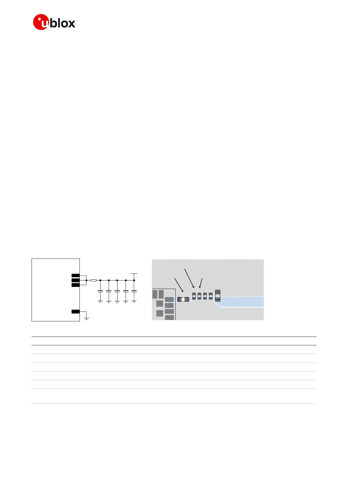
Three pins are allocated to VCC supply connection. Several pins are designated for GND connection.
It is recommended to correctly connect all of them to supply the module minimizing series resistance.
To reduce voltage ripple and noise, improving RF performance especially if the application device
integrates an internal antenna, place the following bypass capacitors near the VCC pins:
• 68 pF capacitor with self-resonant frequency in the 700/800/900 MHz range (e.g. Murata
GRM1555C1H680J), to filter EMI in the low cellular frequency bands
• 15 pF capacitor with self-resonant frequency in the 1700/1800/1900 MHz range (as Murata
GRM1555C1H150J), to filter EMI in the high cellular frequency bands
• 10 nF capacitor (e.g. Murata GRM155R71C103K), to filter digital logic noise from clocks and data
• 100 nF capacitor (e.g. Murata GRM155R61C104K), to filter digital logic noise from clocks and data
An additional capacitor is recommended to avoid undershoot and overshoot at the start and at the
end of RF transmission:
• 10 F capacitor, or greater capacitor, with low ESR (e.g. Murata GRM188R60J106ME47)
An additional series ferrite bead may be provided for additional RF noise filtering, in particular if the
application device integrates an internal antenna:
• Ferrite bead specifically designed for EMI / noise suppression in the GHz frequency band (e.g. the
Murata BLM18EG221SN1), placed as close as possible to the VCC input pins of the module,
implementing the circuit described in Figure 28, to filter out EMI in all the cellular bands

 Loading...