UNION SWITCH & SIGNAL GENISYS II System Hardware Installation
2-8 August 1999 SM-6900B Rev. 0.0
T
ABLE
2-1. C
ARDFILE
M
OTHERBOARD
K
EYING
P
LUG
L
OCATIONS
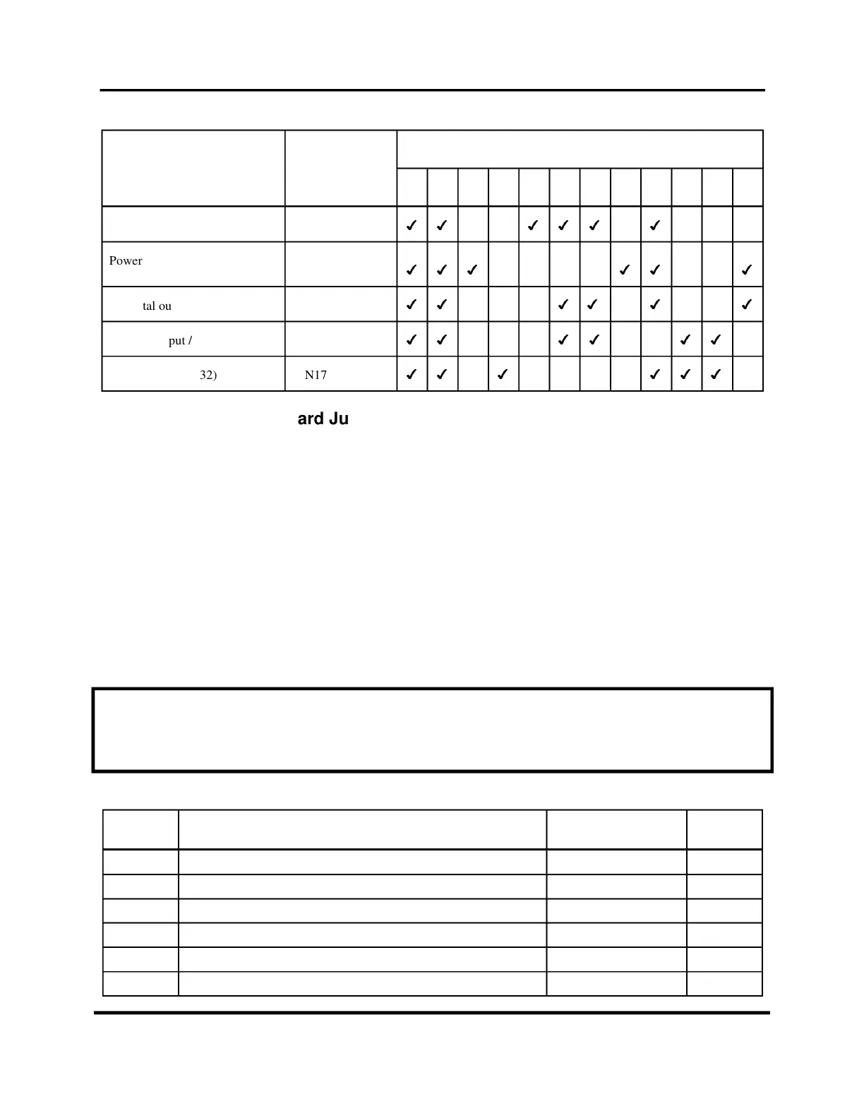
Keying Plug Location (Figure 2-4)
Printed Circuit Board Part No. 123456789101112
CPU N17061310
Power supply N17063001
non-vital output N17062701
non-vital input / LCP driver N17002801
non-vital I/O (32/32) N17061501
2.2.3 Printed Circuit Board Jumper and Firmware Configurations
Two types of GENISYS II printed circuit boards contain jumpers and firmware that must be
configured before each board is installed. These boards are the CPU board and the power supply
board.
2.2.3.1
Configuring the CPU Board
2.2.3.1.1 Jumper Settings (See Figure 2-5)
Prior to installing the CPU board in the GENISYS II cardfile, the following jumpers should be
checked to make certain they are in their proper positions per the system application logic
software or factory requirements.
NOTE
BOLD FACE LETTERS INDICATE BASIC OPERATION WITH THE 21 MHZ
SYSTEM CLOCK.
T
ABLE
2-2. CPU B
OARD
J
UMPER
P
OSITIONS
Jumper
ID
Description Position Notes
JMP1 Bottom PCMCIA 2 Wait States Position 2-3
JMP2 Not installed
JMP3 On-Board RAM 1 Wait State Position 2-3 1
JMP4 Top PCMCIA 2 Wait States Position 2-3
JMP5 Not installed
JMP6 FLASH 1 Wait State Position 2-3 1
 Loading...