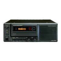
VXR-9000 UHF Service Manual
squelch threshold level to that which is memorized in EE-
PROM Q3006 (BR24L32F) or set by the front panel SQL
control.
RX PLL AND VCO CIRCUITS
The receiver’s PLL circuitry consists of PLL subsystem IC
Q1052 (MB15A02PFV1) on the MAIN Unit, which con-
tains a reference oscillator/divider, serial-to-parallel data
latch, programmable divider, phase comparator and a
swallow counter. Stability is obtained by a regulated 5
VDC supply via Q1062 (L78M05T) and temperature com-
pensated 14.4 MHz crystal oscillator X1003.
The RX VCO made up two VCO circuit, one is Low-Band
RX VCO, consisting of FET Q1048 (2SK508) and varactor
diodes D1018 and D1019 (both 1SV282), and another one
is High-Band RX VCO, consisting of FET Q1049 (2SK508)
and varactor diodes D1020 and D1021 (both 1SV282), os-
cillates between 376.65 MHz and 416.65 MHz according to
the programmed receiving frequency. The RX VCO out-
put passes through buffer amplifier Q1059 (2SC5226) and
first local amplifier Q1019 (2SC3357) to the first mixer
Q1018 (SPM5001), as described previously. A portion of
the RX VCO output is applied to the prescaler/swallow
counter section in the PLL IC Q1052 (MB15A02PFV1).
There the RX VCO signal is divided by 64 or 65, according
to a control signal from the Main CPU Q3014 (HD64F2238)
on the CNTL Unit, before being applied to the program-
mable divider section of the PLL IC Q1052
(MB15A02PFV1).
The data latch section of the PLL IC Q1052
(MB15A02PFV1) also receives serial dividing data from
the Main CPU Q3014 (HD64F2238), which causes the pre-
divided RX VCO signal to be further divided by 75,330 ~
81,330 (or 60,264 ~ 65,064) in the programmable divider
section in the PLL IC Q1052 (MB15A02PFV1), depend-
ing upon the desired receive frequency, so as to produce
a 5 kHz (or 6.25 kHz) derivative of the current RX VCO
frequency. Meanwhile, the reference divider section of the
PLL IC Q1052 (MB15A02PFV1) divides the 14.4 MHz
crystal reference from the reference oscillator X1003 and
Q1045 (2SC4116GR) by 2880 (or 2304) to produce the 5
kHz (or 6.25 kHz) loop reference.
The 5 kHz or 6.25 kHz signal from the programmable di-
vider (derived from the RX VCO) and that derived from
the crystal are applied to the phase detector section of the
PLL IC Q1052 (MB15A02PFV1), which produces a pulsed
output with pulse duration depending on the phase dif-
ference between the input signals. This pulse train is then
converted to DC, low pass filtered, then fed back to the
RX VCO varactor diodes D1018/D1019 and D1020/D1021
(all 1SV282).
Changes in the DC voltage applied to the varactor diodes
D1018/D1019 and D1020/D1021 (all 1SV282) affect the
reactance in the tank circuit RX VCO Q1048/1049 (both
2SK508), changing the oscillating frequency according to
the phase difference between the signals derived from the
RX VCO and the crystal reference oscillator. The RX VCO
is thus phase-locked to the reference frequency standard.
TRANSMIT SIGNAL PATH
The speech audio from the CNTL Unit is applied to the
varactor diode D1010 (HVU350), which frequency mod-
ulates the TX VCO from the unmodulated carrier at the
transmit frequency. The modulated transmit signal is buff-
ered by Q1026 (2SC5226), then passes through the RF
amplifier Q1030 (2SC3357) and RF diode switch D1016
(RN739F) to the PA Unit.
The transmit signal is applied to the RF amplifier Q5001
(2SC3357) and Q5008 (PD55008), then finally amplified
by power amplifier Q5015 and Q5016 (both PD55025S)
up to 50 Watts. Harmonic and spurious radiation in the
final output is suppressed by a low pass filter consisting
of coils L5007 ~ L5010, plus capacitors C5071, C5078,
C5082, C5085, and C5088 on the PA Unit, before delivery
to the TX antenna jack.
TX PLL AND VCO CIRCUITS
The Transmitter’s PLL circuitry consists of PLL subsystem
IC Q1008 (MB15A02PFV1) on the MAIN Unit, which con-
tains a reference oscillator/divider, serial-to-parallel data
latch, programmable divider, phase comparator and a
swallow counter. Stability is obtained by a regulated 5
VDC supply via Q1062 (L78M05T) and temperature com-
pensated 14.4 MHz crystal oscillator X1001.
The TX VCO, consisting of FET Q1021 (2SK508) and var-
actor diodes D1008 and D1009 (both 1SV282), oscillates
between 450 MHz and 490 MHz according to the pro-
grammed transmit frequency. The theory of operation of
the remainder of the PLL circuitry is similar to that of the
RX PLL circuit; however, dividing data from the Main
CPU Q3014 (HD64F2238) on the CNTL Unit is such that
the VCO frequency is the actual transmit frequency.
APC
(
AUTOMATIC POWER CONTROL
)
RF power output from the final amplifier Q5015/Q5016
(both PD55025S) is sampled by C5061/C5056 and is then
rectified by D5007 and D5008 (both HSM88AS). The re-
sulting DC voltage is applied to the comparator Q5005
(TA75S01F), where the voltage is compared with a refer-
ence voltage from the Main CPU Q3014 (HD64F2238) on
the CNTL Unit, to produce a control voltage for the Auto-
matic Power Controller Q5004 (2SC4116GR) and Q5002
(2SB1122S), which regulates supply voltage to Q5001
(2SC3357).
Circuit Description
F-2
 Loading...