AC701 Getting Started Guide www.xilinx.com 19
UG967 (v3.0) July 10, 2013
Advanced Bring-up with Base Targeted Reference Design
Advanced Bring-up with Base Targeted Reference Design
Introduction
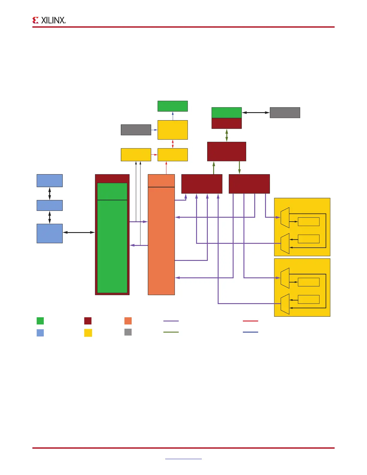
Figure 14 depicts the block-level overview of the Artix-7 FPGA base Targeted Reference
Design (TRD) which delivers up to 10 Gb/s of performance per direction.
X-Ref Target - Figure 14
Figure 14: Artix-7 FPGA Base TRD Block Diagram
GUI
XDMA
Driver
XRaw Driver
PCIe x4
Gen2 Link
PCIe IP
GTP
Transceiver
PCIe
Integrated
Endpoint
Block x4 Gen2
AXI Target
Master
Packet
DMA
512 bits at
100 MHz
PCIe
Monitor
User Space
Registers
UG967_14_121912
AXI Stream Generator
and Checker
Generator
Checker
Loopback
AXI Stream Generator
and Checker
Generator
Checker
Loopback
XADC
64 x 250 MHz 64 x 250 MHz
AXIS IC
S0 S1 S2 S3
AXIS IC
M3 M2 M1 M0
AXI VFIFO
WR RD
AXI MIG
DDR3 IO
DDR3
S2C0
C2S0
S2C1
C2S1
Power and
Temperature
Monitor
UCD90120A
512 bits at
100 MHz
512 bits at
100 MHz
64 bits at
800 Mb/s
128 bits at
125 MHz
128 bits at
125 MHz
128 bits at
125 MHz
128 bits at
125 MHz
Integrated Blocks
in FPGA
Xilinx IP
Third Party IP
Custom RTL
Software Driver
On Board
AXI ST (128 bits at 125 MHz)
AXI MM (512 bits at 100 MHz)
Control Path
50 MHz Domain

 Loading...


