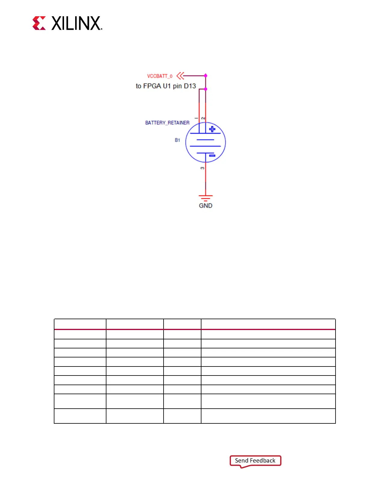
Figure 3: Encryption Key Backup Circuit
The Keystone 2998 baery retainer B1 is soldered to the board with the posive output
connected to the FPGA U1 VCC_PSBATT pin D13. The B1 retainer accepts a 6.8 mm 1.5V
single-cell, coin type baery similar to Seiko part number SR621SW, silver oxide, 1.55V non-
rechargeable baery.
Bank Voltage Rails
The XC7S100 FPGA U1 bank voltages are listed in the following table.
Table 7: FPGA U1 Bank Voltage Rails
XC7S100 U1 Bank Power Net Name Voltage Connected To
0 VCCO_3V3 3.3V FPGA Configuration I/F
13 VCCO_1V8 1.8V MIPI_DSI, GPIO Switches, FT4232_C_UART, I2C3_DSI Bus
14 VCCO_3V3 3.3V FLASH_SPI, FT4232_B_UART
15 VCCO_3V3 3.3V HDMI Out, I2C4_HDMI Bus, GPIO LEDs, XADC I/F
16 VCCO_3V3 3.3V PMOD[1:6] I/F
33 VCCO_2V5 2.5V Ethernet PHY 1/2 I/F, MIPI_CSI, I2C2_CAM
34 VCCO_1V35 1.35V DDR3L I/F
35 VADJ 1.8V (nom),
3.3V, 2.5V
LPC FMC I/F, MPS430_GPIO
36 VADJ 1.8V (nom),
3.3V, 2.5V
LPC FMC I/F, MPS430_GPIO
Chapter 3: Board Component Descriptions
UG1319 (v1.0) July 12, 2019 www.xilinx.com
SP701 Board User Guide 16