EasyManua.ls Logo

Yaesu FT-2000/D User Manual

Yaesu FT-2000/D
220 pages
To Next Page IconTo Next Page
Page #1 background imageLoading...
Page #1 background image
Introduction
This manual provides technical information necessary
for servicing the FT-2000/D HF/50 MHz Transceiver.
Servicing this equipment requires expertise in handling
surface-mount chip components. Attempts by non-qual-
ified persons to service this equipment may result in per-
manent damage not covered by the warranty, and may
be illegal in some countries.
Two PCB layout diagrams are provided for each double-
sided circuit board in the Transceiver. Each side of is re-
ferred to by the type of the majority of components in-
stalled on that side (“leaded” or “chip-only”). In most
cases one side has only chip components, and the other
has either a mixture of both chip and leaded components
(trimmers, coils, electrolytic capacitors, ICs, etc.), or lead-
ed components only.
While we believe the technical information in this man-
ual to be correct, VERTEX STANDARD assumes no lia-
bility for damage that may occur as a result of typograph-
ical or other errors that may be present. Your coopera-
tion in pointing out any inconsistencies in the technical
information would be appreciated.
©2007 VERTEX STANDARD CO., LTD. EH025H90B
Technical Supplement
HF/50 MHz TRANSCEIVER
FT-2000/D
Contents
Specifications
Exploded View & Miscellaneous Parts
Block Diagram
Connection Diagram
Alignment
Board Unit (Schematics, Layouts & Parts)
MAIN Unit
VRF Unit
BPF Unit
ANT Unit
DVS Unit
CNTL Unit
LOCAL Unit
RX-2 Unit
PA-A Unit
PA-B Unit
TUNER-MAIN Unit
TUNER-CNTL Unit
DSP Unit
VR-A Unit
VR-B Unit
SW-A Unit
MIC Unit
JACK Unit
KEY Unit
BACK-LIGHT Unit
F-CONNECT Unit
VERTEX STANDARD CO., LTD.
4-8-8 Nakameguro, Meguro-Ku, Tokyo 153-8644, Japan
VERTEX STANDARD
US Headquarters
10900 Walker Street, Cypress, CA 90630, U.S.A.
YAESU EUROPE B.V.
P.O. Box 75525, 1118 ZN Schiphol, The Netherlands
YAESU UK LTD.
Unit 12, Sun Valley Business Park, Winnall Close
Winchester, Hampshire, SO23 0LB, U.K.
VERTEX STANDARD HK LTD.
Unit 5, 20/F., Seaview Centre, 139-141 Hoi Bun Road,
Kwun Tong, Kowloon, Hong Kong
VERTEX STANDARD
(
AUSTRALIA
)
PTY., LTD.
Normanby Business Park, Unit 14/45 Normanby Road
Notting Hill 3168, Victoria, Australia
Question and Answer IconNeed help?

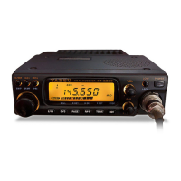
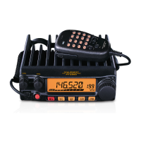
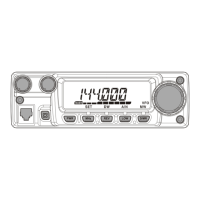
Do you have a question about the Yaesu FT-2000/D and is the answer not in the manual?

Yaesu FT-2000/D Specifications

General IconGeneral
BrandYaesu
ModelFT-2000/D
CategoryTransceiver
LanguageEnglish

Summary

Introduction

Specifications

General Specifications

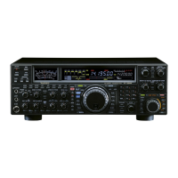
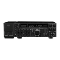
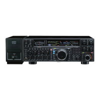
General operational parameters and characteristics of the transceiver.

Transmitter Specifications

Parameters related to the transmitter's performance and capabilities.

Receiver Specifications

Parameters related to the receiver's performance and sensitivity.

FP-2000 Power Supply Specifications

Specifications for the external power supply unit.

Exploded View

Case Assembly

Exploded view of the transceiver's outer case and legs.

Panel Assembly

Exploded view of the front panel components and knobs.

Chassis Assembly

Exploded view of the main chassis and internal units.

Block Diagram

Connection Diagram

Alignment Procedures

Introduction and Precautions

Important safety and preparation guidelines before performing alignment.

Required Test Equipment

List of necessary tools and instruments for transceiver alignment.

Analog Meter Adjustment

Procedure for adjusting the main S-meter for full scale deflection.

2nd Local Oscillator (Main) Adjustment

Alignment procedure for the main unit's 2nd local oscillator frequency.

1st Local Oscillator Adjustment

Alignment procedure for the main unit's 1st local oscillator.

IF Transformer Adjustment

Procedure for adjusting IF transformers for optimal signal processing.

Noise Blanker Circuit Adjustment

Alignment procedure for the noise blanker circuit.

RF AGC Adjustment

Procedure for adjusting the RF Automatic Gain Control.

PA-A Unit (100 W Type) Adjustment

Alignment procedures specific to the 100W Power Amplifier A unit.

PA-B Unit Adjustment

Alignment procedures specific to the 200W Power Amplifier B unit.

Antenna Tuner Adjustment

Procedures for adjusting the antenna tuner circuit for optimal performance.

Transmitter Section Alignment Mode

Procedures for alignment within the transmitter section.

Power Adjustment

Procedure for setting the transceiver's output power levels.

MAIN Unit

Circuit Diagram

Schematic diagram of the MAIN Unit's electronic circuitry.

Parts Layout (Side A)

Physical placement of components on the MAIN Unit's Side A PCB.

VRF Unit

Circuit Diagram

Schematic diagram of the VRF Unit's electronic circuitry.

Parts Layout

Physical placement of components on the VRF Unit's PCB.

BPF Unit

Circuit Diagram

Schematic diagram of the BPF Unit's electronic circuitry.

Parts Layout

Physical placement of components on the BPF Unit's PCB.

ANT Unit

Circuit Diagram

Schematic diagram of the ANT Unit's electronic circuitry.

Parts Layout (Side A)

Physical placement of components on the ANT Unit's Side A PCB.

DVS Unit

Circuit Diagram

Schematic diagram of the DVS Unit's electronic circuitry.

Parts Layout

Physical placement of components on the DVS Unit's PCB.

CNTL Unit

Circuit Diagram

Schematic diagram of the CNTL Unit's electronic circuitry.

Parts Layout (Side A)

Physical placement of components on the CNTL Unit's Side A PCB.

LOCAL Unit

Circuit Diagram

Schematic diagram of the LOCAL Unit's electronic circuitry.

Parts Layout (Side A)

Physical placement of components on the LOCAL Unit's Side A PCB.

RX-2 Unit

Circuit Diagram

Schematic diagram of the RX-2 Unit's electronic circuitry.

Parts Layout (Side A)

Physical placement of components on the RX-2 Unit's Side A PCB.

PA-A Unit

Circuit Diagram

Schematic diagram of the PA-A Unit's electronic circuitry.

Parts Layout (Side A)

Physical placement of components on the PA-A Unit's Side A PCB.

PA-B Unit (200 W)

Circuit Diagram

Schematic diagram of the PA-B Unit's electronic circuitry.

Parts Layout (Side A)

Physical placement of components on the PA-B Unit's Side A PCB.

TUNER-MAIN Unit

Circuit Diagram

Schematic diagram of the TUNER-MAIN Unit's electronic circuitry.

Parts Layout (Side A)

Physical placement of components on the TUNER-MAIN Unit's Side A PCB.

TUNER-CNTL Unit

Circuit Diagram

Schematic diagram of the TUNER-CNTL Unit's electronic circuitry.

Parts Layout (Side A)

Physical placement of components on the CNTL Unit's Side A PCB.

DSP Unit

Circuit Diagram

Schematic diagram of the DSP Unit's electronic circuitry.

Parts Layout (Side A)

Physical placement of components on the DSP Unit's Side A PCB.

VR-A Unit

Circuit Diagram

Schematic diagram of the VR-A Unit's electronic circuitry.

Parts Layout (Side A)

Physical placement of components on the VR-A Unit's Side A PCB.

VR-B Unit

Circuit Diagram

Schematic diagram of the VR-B Unit's electronic circuitry.

Parts Layout

Physical placement of components on the VR-B Unit's PCB.

SW-A Unit

Circuit Diagram

Schematic diagram of the SW-A Unit's electronic circuitry.

Parts Layout (Side A)

Physical placement of components on the SW-A Unit's Side A PCB.

MIC Unit

Circuit Diagram

Schematic diagram of the MIC Unit's electronic circuitry.

Parts Layout

Physical placement of components on the MIC Unit's PCB.

JACK Unit

Circuit Diagram

Schematic diagram of the JACK Unit's electronic circuitry.

Parts Layout

Physical placement of components on the JACK Unit's PCB.

KEY Unit

Circuit Diagram

Schematic diagram of the KEY Unit's electronic circuitry.

Parts Layout (Side A)

Physical placement of components on the KEY Unit's Side A PCB.

BACK-LIGHT Unit

Circuit Diagram

Schematic diagram of the BACK-LIGHT Unit's electronic circuitry.

Parts Layout

Physical placement of components on the BACK-LIGHT Unit's PCB.

F-CONNECT Unit

Circuit Diagram

Schematic diagram of the F-CONNECT Unit's electronic circuitry.

Parts Layout

Physical placement of components on the F-CONNECT Unit's PCB.

Related product manuals