CB81
CB83
CB84
CB85
CB87
CB88
CB89
CB90
IC81
IC82
IC83
A
1
2
3
4
5
6
7
8
9
10
BCDEFGH I JK
L MN
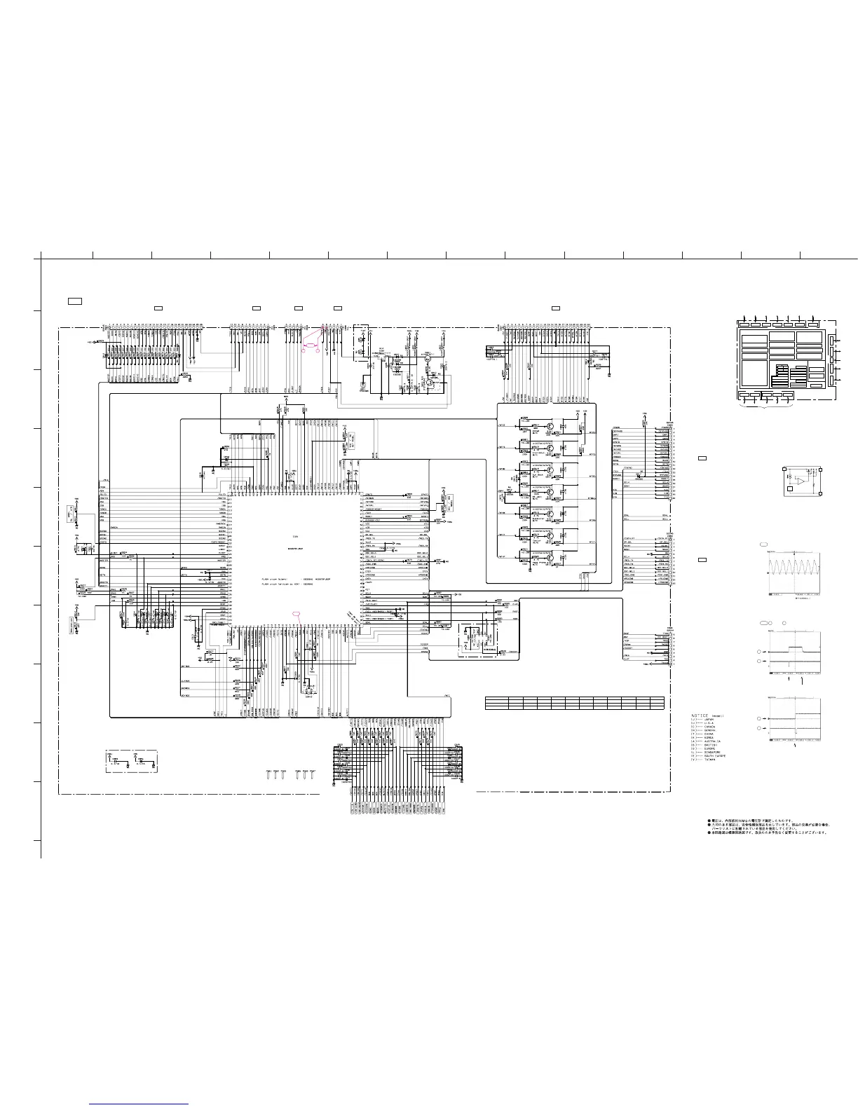
RX-V661/HTR-6060/DSP-AX761
95
★ All voltages are measured with a 10MΩ/V DC electronic voltmeter.
★ Components having special characteristics are marked s and must be replaced
with parts having specifications equal to those originally installed.
★ Schematic diagram is subject to change without notice.
DSP 3/3
2
C-1
1
B-2
POINT C-1 1 / Pin5, 2 / Pin6 of CB85
AC cable ON
AC cable OFF
+5M
/RES
1
2
1
2
AC cable ON
POINT B-2 Pin 20 of IC81
4.94.4
0
0
0
0.1
4.9
0.1
4.9
4.9
0.1
4.9
0.1
4.9
4.9
0
0.1
0
0
4.8
4.9
5.0
5.1
4.9
5.2
0
4.9
0.1
0.1
0
0
5.0
5.0
5.0
5.0
5.0
4.9
4.9
0
0.2
0
0
0
4.9
0
4.5
4.5
4.5
4.8
0
4.9
0.4
4.9
0.1
0
0
0
4.9
4.9
4.9
0
0
4.9
0
0.1
0
4.9
4.9
4.9
4.9
0.1
0.1
5.0
0
0
4.7
5.2
0.5
5.1
0
1.0
1.0
4.9
5.1
4.9
0
4.9
2.3
3.2
5.2
5.2
4.9
4.9
0
0.1
0
5.2
4.8
4.9
4.9
0.1
4.9
5.0
0
0.1
0
0
2.4
0
2.5
4.9
5.0
5.0
4.9
4.9
4.9
0
0
0.1
5.0
2.7
0
0.2
4.9
4.8
4.8
0
4.7
5.2
0
4.8
0
4.9
5.0
0
4.9
5.1
10.1
0
5.8
5.8
5.8
5.8
5.1
5.1 5.1
5.1
4.9
4.8 4.8
0
0
4.4
5.2
5.0
0.1 0.6
4.4
5.1
5.0
4.4
5.1
0.10.6
0.64.8
5.0
4.4
5.1
5.0
4.4
5.1
5.0
4.9
5.1
-11.9
4.9
5.1
-11.9
4.9
5.1
-6.6
0.5
3.2
0
0
2.3
5.15.1
IC81: M30878JBGP
Single chip 16/32-bit microprocessor
Port P0 Por t P1 Port P2 Por t P3 Por t P4 Port P5 Por t P6
Port P7
Port P14 Por t P15 Port P11 Port P12
Port P10Po rt P9Port P8
P85
Port P13
R0H R0L
R1H R1L
R2
R3
A0
A1
FB
SB
NOTES:
1. Ports P11 to P15 are provided in the 144-pin package only.
2. Included in the 144-pin package only. 26 inputs maximum in the 100-pin package.
3. 6 channes available in the 100-pin package.
4. 6 channes available in the 100-pin package.
5. 10 channes available in the 100-pin package.
FLG
INTB
ISP
USP
PC
SVF
SVP
VCT
Multiplier
M32C/80 series mixroprocerssor Core
Clock Generation Circuit
XIN - XOUT
XCIN - XCOUT
On-chip Oscillator
PLL Frequency Synthesizer
A/D Converter:
1 circuit
Standard: 10 inputs
Maximum: 34 inputs
(2)
UART/Clock Synchronous Serial I/O:
7 channels
(3)
CRC Calculation Circuit (CCITT):
X
16
+X
12
+X
5
+1
X/Y Converter:
16 bits x 16 bits
D/A Converter:
8 bits x 2 channels
Peripher al Functions
<VCC2>
<
VCC1>
<VCC1>
ROM
RAM
Memory
<VCC1>
<VCC2>
78 58 8
(Note 1)
8
8
7
888888 8
8
DMACII
DMAC
Watchdog Ti mer (15 bits)
CAN Module: 2 channel
Intelligent I/O
Time Measur ement: 8 channe ls
(4)
Wave Generating: 16 channels
(5)
Communication Functions:
Clock Synchronous Serial I/O, UART,
HDLC Data Processing
Timer (16 bits)
Timer A: 5 channels
Timer B: 6 channels
Three-Phase Motor Control Circuit
2
1
3
VOUT
GND
V
IN
–
+
IC82: RH5RE58AA-T1-FA
Voltage regulator
Vref
DSP
s103
s102
s101
s100
MICROPROCESSOR
Pull-up resistance 10 k-ohms
Destination detection for AD port
Ohm (R815)
V
A/D (5 V=255)
DEST, 139 pin
0.0 k
0 - 0.3
0 - 13
J
1.2 k
0.4 - 0.7
14 - 40
U, C
2.7 k
0.8 - 1.3
41 - 68
–
4.7 k
1.4 - 1.8
69 - 92
R
6.8 k
1.9 - 2.2
93 - 115
T
15.0 k
2.8 - 3.2
141 - 170
A
27.0 k
3.3 - 3.8
171 - 198
B
47.0 k
3.9 - 4.3
199 - 221
G, E
100.0 k
4.4 - 4.7
222 - 243
L
–
4.8 - 5.0
245 - 255
–
10.0 k
2.3 - 2.7
116 - 140
K
to OPERATION (1)_CB401
Page 98
F9
to MAIN (1)_W103
Page 99 H5
to MAIN (1)_W104
Page 99 H4
to FUNCTION (3)_W2501
R model
Page 97 G8
to FUNCTION (1)_CB206
Page 96 B8
to VIDEO_CB303
Page 100
D2
to HDMI_CB5
WRITING PORT
Page 101
L6
to DSP 1/3
 Loading...