EasyManua.ls Logo

Yamaha HTR-5740 - Service Manual

Yamaha HTR-5740
125 pages
Print Icon
To Next Page IconTo Next Page
Loading...
SERVICE MANUAL
100884
IMPORTANT NOTICE
This manual has been provided for the use of authorized YAMAHA Retailers and their service personnel.
It has been assumed that basic service procedures inherent to the industry, and more specifically YAMAHA Products, are already
known and understood by the users, and have therefore not been restated.
WARNING: Failure to follow appropriate service and safety procedures when servicing this product may result in personal
injury, destruction of expensive components, and failure of the product to perform as specified. For these reasons,
we advise all YAMAHA product owners that any service required should be performed by an authorized
YAMAHA Retailer or the appointed service representative.
IMPORTANT: The presentation or sale of this manual to any individual or firm does not constitute authorization, certification or
recognition of any applicable technical capabilities, or establish a principle-agent relationship of any form.
The data provided is believed to be accurate and applicable to the unit(s) indicated on the cover. The research, engineering, and
service departments of YAMAHA are continually striving to improve YAMAHA products. Modifications are, therefore, inevitable
and specifications are subject to change without notice or obligation to retrofit. Should any discrepancy appear to exist, please
contact the distributor's Service Division.
WARNING: Static discharges can destroy expensive components. Discharge any static electricity your body may have
accumulated by grounding yourself to the ground buss in the unit (heavy gauge black wires connect to this buss).
IMPORTANT: Turn the unit OFF during disassembly and part replacement. Recheck all work before you apply power to the unit.
P.O.Box 1, Hamamatsu, Japan
CONTENTS
TO SERVICE PERSONNEL .......................................... 2
IMPEDANCE SELECTOR ............................................. 3
FRONT PANELS ........................................................ 4~6
REAR PANELS ........................................................ 7~15
REMOTE CONTROL PANELS .................................... 16
SPECIFICATIONS / 参考仕様 ................................ 17~18
INTERNAL VIEW ......................................................... 18
DISASSEMBLY PROCEDURES/分解手順 ......... 19~21
SELF DIAGNOSIS FUNCTION (DIAG)/
自己診断機能(ダイアグ)..................................... 22~42
AMP ADJUSTMENT/アンプ部調整 ........................... 43
IC DATA ................................................................. 44~49
BLOCK DIAGRAM ................................................. 50~51
DISPLAY DATA ........................................................... 52
PRINTED CIRCUIT BOARD .................................. 53~73
PIN CONNECTION DIAGRAM .................................... 74
SCHEMATIC DIAGRAM ........................................ 75~85
PARTS LIST ......................................................... 87~123
REMOTE CONTROL.......................................... 124~125
AV RECEIVER/AV AMPLIFIER
RX-V550/HTR-5750
RX-V450/HTR-5740/DSP-AX450
RX-V550/HTR-5750
RX-V450/HTR-5740/DSP-AX450

Other manuals for Yamaha HTR-5740

Question and Answer IconNeed help?

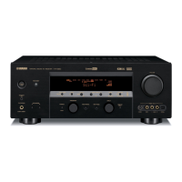
Do you have a question about the Yamaha HTR-5740 and is the answer not in the manual?

Summary

TO SERVICE PERSONNEL

Critical Components Information

Information on critical components requiring specific replacement parts.

Leakage Current Measurement

Procedure and limits for verifying insulation after service.

CHEMICAL CONTENT NOTICE!

Warning about lead and other chemicals in product components.

IMPEDANCE SELECTOR

About Lead Free Solder

Information on lead-free solder types and cautionary notes for repair.

FRONT PANELS

REAR PANELS

REMOTE CONTROL PANELS

SPECIFICATIONS

INTERNAL VIEW

DISASSEMBLY PROCEDURES

1. Removal of Top Cover

Steps for removing the top cover of the unit.

2. Removal of Front Panel Unit

Steps for removing the front panel unit.

3. Removal of Plate Side

Steps for removing the side plate.

4. Removal of Sub Chassis Unit

Steps for removing the sub-chassis unit.

5. Removal of DSP P.C.B.

Steps for removing the DSP P.C.B.

6. Removal of FUNCTION (1) ~ (8) P.C.B.s and Tuner

Steps for removing various FUNCTION P.C.B.s and the tuner.

SELF DIAGNOSIS FUNCTION (DIAG)

Starting DIAG

Procedure for initiating the diagnostic mode using main unit keys.

Starting DIAG in the protection cancel mode

Procedure to start DIAG with protection functions disabled.

Canceling DIAG

Steps to exit diagnostic mode and reset settings.

Display provided when DIAG started

What the FL display shows when DIAG mode is initiated.

When there is no history of protection function

Expected display when no protection events have occurred.

When there is a history of protection function

Information on display when protection events are logged.

When there is a history of protection function due to abnormal DC output

Display for abnormal DC output protection history.

History of protection function

How protection history is stored and cleared.

Display during menu operation

How the FL indicator shows active functions during DIAG.

Operation procedure of DIAG menu and SUB-MENU

How to navigate DIAG menus and sub-menus using main unit keys.

Functions in DIAG mode

Available functions during DIAG mode operation, excluding tuner/menu.

Initial settings used to start DIAG

Default settings applied when entering DIAG mode.

Details of DIAG menu

2. BYPASS

ANALOG BYPASS

Signal bypass through L/R without DSP processing.

DSP BYPASS

Signal bypass through the DSP section.

3. RAM THROUGH

RAM MARGIN

Selecting full-bit output at 0dB level for analog and PCM signals.

RAM FULL BIT

Selecting full-bit output at 0dB level for analog and PCM signals.

4. PRO LOGIC

PRO LOGIC I

Selecting PRO LOGIC I mode; Auto Input Balance is off.

PRO LOGIC II

Selecting PRO LOGIC II mode; Auto Input Balance is off.

Neo:6

5. SPEAKERS SET

LARGE

Mode for speakers with high bass performance; full bandwidth output.

SMALL

Mode for speakers with low bass performance; signals mixed into LFE/BASS.

NONE

Mode when no speakers are used; center reduced and distributed to MAIN L/R.

6. EXTERNAL INPUT

6 ch INPUT_6

Outputting signal from 6CH INPUT terminals with 6-ohm speaker impedance selection.

6 ch INPUT_8

Outputting signal from 6CH INPUT terminals with 8-ohm speaker impedance selection.

7. MIC CHECK

MIC CHK -dB

Microphone check function, not applicable to these models.

8. DISPLAY CHECK

Initial display

Checking the initial display of the FL section.

All segments OFF

Checking FL driver by turning off all segments.

All segments ON (dimmer 100%)

Checking FL driver by turning on all segments at 100% dimmer.

All segments ON (dimmer 50%)

Checking FL driver by turning on all segments at 50% dimmer.

Lighting of segments in lattice

Checking for segment shorts by lighting segments alternately.

9. MANUAL TEST

TEST ALL

Outputting noise from all channels.

TEST MAIN L

Outputting noise from the FRONT L channel.

TEST CENTER

Outputting noise from the CENTER channel.

TEST MAIN R

Outputting noise from the FRONT R channel.

TEST REAR L

Outputting noise from the SURROUND L channel.

TEST REAR R

Outputting noise from the SURROUND R channel.

TEST REAR CENTER

Outputting noise from the SURROUND BACK L channel.

TEST SB R

Outputting noise from the SURROUND BACK R channel.

TEST LFE

Outputting noise from the SUB WOOFER channel.

10. FACTORY PRESET

PRESET INHIBIT (Initialization inhibited)

Prevents RAM initialization; protects user settings.

PRESET RESERVED (Initialization reserved)

Reserves RAM initialization for resetting settings.

11. AD DATA CHECK

DC;PS (protection detection)

Detects DC output and power supply voltage protection values.

THM;Fan (temperature detection;fan drive level)

Detects temperature and fan drive levels.

IMP SW;POWER LIMIT

K0;K1 (Panel key of main unit)

12. V CONV STATUS

13. IF STATUS (Input function status)

<1 st byte> Digital input;output setting value

Displays REC OUT and INPUT selection status.

<2 nd byte> Fs information of reproduction signal

Shows reproduction signal frequency information.

<3 rd byte> Audio code mode information of reproduction signal

Indicates audio code mode for reproduction signals.

<4 th byte> Format information of reproduction signal

Provides format information for reproduction signals.

<5 th byte> Signal processing status information

14. DSP RAM CHECK

YSS930 Bus Check

Checks bus connection for YSS930 and external RAM.

YSS948 BUS CHECK

Checks bus connection for YSS948 and external RAM.

15. PROTECTION SETTING

16. SOFT SW

SW MODE: PCB or SOFT

Selects software mode for PCB settings.

MODEL SETTING

Allows selection of the unit's model setting.

TUNER DESTINATION

Sets the tuner destination region.

TUNER

Tuner setting option.

RDS

RDS setting option.

ZONE2

Zone 2 setting option.

VIDEO FORMAT

Sets the video format to NTSC or PAL.

17. MICROPROCESSOR INFORMATION

Version

Displays software version information.

Checksum

Displays checksum for program areas.

Check of port setting for judging microprocessor function

Checks port settings for microprocessor function.

Display of AAC function detection port state

Shows the state of AAC function detection ports.

AMP ADJUSTMENT

Confirmation of Idling Current of MAIN (1) P. C. B.

Measures and confirms idling current for the MAIN (1) P.C.B. terminals.

Attention

Cautionary note for checking defective components before cutting bias resistors.

IC DATA

Block name

Lists block names within the IC.

Function

Describes the function of each block.

PIN CONNECTION DIAGRAM

Function Check Table

Table correlating pin functions with settings and remarks.

BLOCK DIAGRAM (1;2)

BLOCK DIAGRAM (2;2)

DISPLAY DATA

ANODE CONNECTION

Diagram showing anode connections for the FL display.

PIN CONNECTION

Lists pin assignments for the FL display driver.

GRID ASSIGNMENT

Shows grid assignments for the FL display.

PRINTED CIRCUIT BOARD (Foil side)

Semiconductor Location

Indicates locations of semiconductors on the PCB.

PRINTED CIRCUIT BOARD (Foil side)

Semiconductor Location

Indicates locations of semiconductors on the PCB.

PRINTED CIRCUIT BOARD (Foil side)

Semiconductor Location

Indicates locations of semiconductors on the PCB.

PRINTED CIRCUIT BOARD (Foil side)

Semiconductor Location

Indicates locations of semiconductors on the PCB.

PRINTED CIRCUIT BOARD (Foil side)

Semiconductor Location

Indicates locations of semiconductors on the PCB.

PRINTED CIRCUIT BOARD (Foil side)

Semiconductor Location

Indicates locations of semiconductors on the PCB.

PRINTED CIRCUIT BOARD (Foil side)

Semiconductor Location

Indicates locations of semiconductors on the PCB.

PRINTED CIRCUIT BOARD (Foil side)

Semiconductor Location

Indicates locations of semiconductors on the PCB.

PRINTED CIRCUIT BOARD (Foil side)

Semiconductor Location

Indicates locations of semiconductors on the PCB.

PRINTED CIRCUIT BOARD (Foil side)

Semiconductor Location

Indicates locations of semiconductors on the PCB.

PRINTED CIRCUIT BOARD (Foil side)

Semiconductor Location

Indicates locations of semiconductors on the PCB.

PRINTED CIRCUIT BOARD (Foil side)

Semiconductor Location

Indicates locations of semiconductors on the PCB.

PRINTED CIRCUIT BOARD (Foil side)

Semiconductor Location

Indicates locations of semiconductors on the PCB.

PRINTED CIRCUIT BOARD (Foil side)

Semiconductor Location

Indicates locations of semiconductors on the PCB.

PRINTED CIRCUIT BOARD (Foil side)

Semiconductor Location

Indicates locations of semiconductors on the PCB.

PRINTED CIRCUIT BOARD (Foil side)

Semiconductor Location

Indicates locations of semiconductors on the PCB.

PRINTED CIRCUIT BOARD (Foil side)

Semiconductor Location

Indicates locations of semiconductors on the PCB.

PRINTED CIRCUIT BOARD (Foil side)

Semiconductor Location

Indicates locations of semiconductors on the PCB.

PRINTED CIRCUIT BOARD (Foil side)

Semiconductor Location

Indicates locations of semiconductors on the PCB.

PRINTED CIRCUIT BOARD (Foil side)

Semiconductor Location

Indicates locations of semiconductors on the PCB.

PRINTED CIRCUIT BOARD (Foil side)

Semiconductor Location

Indicates locations of semiconductors on the PCB.

PIN CONNECTION DIAGRAM

Function Check Table

Table correlating pin functions with settings and remarks.

SCHEMATIC DIAGRAM (DSP)

SCHEMATIC DIAGRAM (FUNCTION 1;2)

SCHEMATIC DIAGRAM (FUNCTION 2;2)

SCHEMATIC DIAGRAM (FUNCTION 1;2) HTR-5750

SCHEMATIC DIAGRAM (FUNCTION 2;2) HTR-5750

SCHEMATIC DIAGRAM (OPERATION) RX-V550

SCHEMATIC DIAGRAM (OPERATION) HTR-5750

SCHEMATIC DIAGRAM (MAIN)

SCHEMATIC DIAGRAM (POWER)

SCHEMATIC DIAGRAM (SUBTRANS)

SCHEMATIC DIAGRAM (VIDEO)

PARTS LIST

ELECTRICAL PARTS

Lists electrical components alphabetically with abbreviations.

P.C.B. MAIN

P.C.B. POWER

P.C.B. POWER & P.C.B. SUBTRANS

P.C.B. POWER

Parts list for the power P.C.B.

P.C.B. SUBTRANS

Parts list for the subtrans P.C.B.

P.C.B. SUBTRANS & P.C.B. VIDEO

P.C.B. SUBTRANS

Parts list for the subtrans P.C.B.

P.C.B. VIDEO

Parts list for the video P.C.B.

CHIP PARTS

EXPLODED VIEW RX-V550

MECHANICAL PARTS RX-V550

EXPLODED VIEW (FRONT PANEL UNIT & SUB CHASSIS UNIT) RX-V550

MECHANICAL PARTS (FRONT PANEL UNIT & SUB CHASSIS UNIT) RX-V550

List of mechanical parts for the front panel and sub chassis.

EXPLODED VIEW (AMP UNIT) RX-V550

MECHANICAL PARTS (AMP UNIT) RX-V550

List of mechanical parts for the amplifier unit.

EXPLODED VIEW (AMP UNIT) HTR-5750 RX-V450;HTR-5740;DSP-AX450

MECHANICAL PARTS HTR-5750 RX-V450;HTR-5740;DSP-AX450

EXPLODED VIEW (FRONT PANEL UNIT) HTR-5750 RX-V450;HTR-5740;DSP-AX450

MECHANICAL PARTS (FRONT PANEL UNIT) HTR-5750 RX-V450;HTR-5740;DSP-AX450

List of mechanical parts for the front panel unit.

EXPLODED VIEW (AMP UNIT) HTR-5750 RX-V450;HTR-5740;DSP-AX450

REMOTE CONTROL: RAV250: RX-V550 (U, C, A, L, R, T, K models), HTR-5750, RX-V450;HTR-5740 (U, C, A, L, R, T, K models), DSP-AX450 RAV251: RX-V550 (B, G, E models)

SCHEMATIC DIAGRAM

Schematic diagram of the remote control circuit.

REMOTE CONTROL RAV302: RX-V450;HTR-5740 (B, G, E models)

SCHEMATIC DIAGRAM

Schematic diagram of the remote control circuit.

Yamaha HTR-5740 Specifications

General IconGeneral
Channels6.1
Dolby DigitalYes
DTSYes
TunerAM/FM
TypeAV Receiver
THD0.06%
Input Sensitivity200 mV/47 kOhms
Signal to Noise Ratio100 dB
Frequency Response10 Hz-100 kHz
Input Impedance47 kOhms
Digital inputs2 Optical, 1 Coaxial
Surround Sound FormatsDolby Digital, DTS, Dolby Pro Logic II
Digital Audio Inputs2 Optical, 1 Coaxial
InputsDigital Optical: 2, Digital Coaxial: 1
Outputs1 Optical Digital
Dimensions435 x 151 x 390 mm
Weight10 kg
Video Inputs/OutputsComposite: 4 in / 2 out
Output Power75W per channel

Related product manuals