6
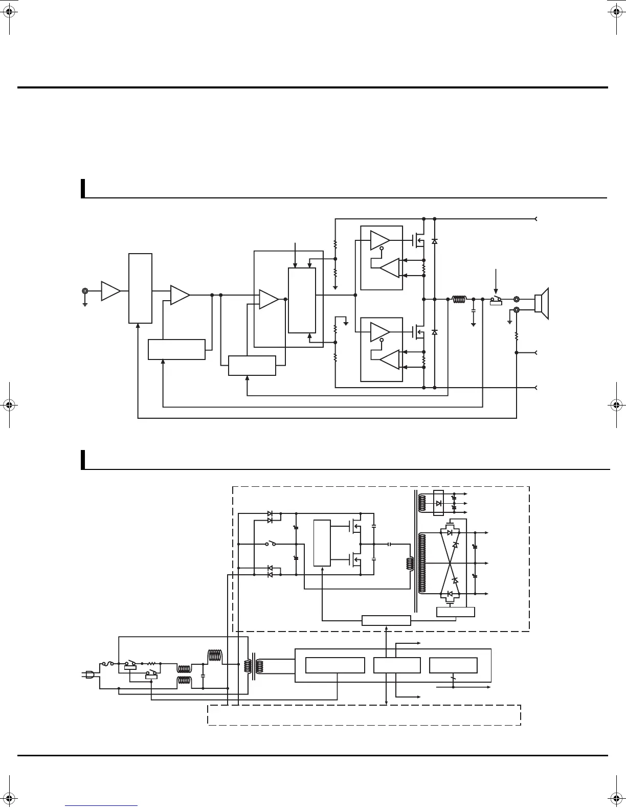
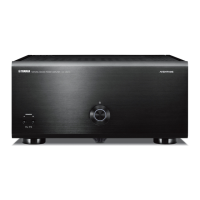
The MX-D1 is a high-power, high-performance PWM (Pulse Width Modulation) digital stereo power amplifier, utilizing
Yamaha’s latest digital power amplifier and switching power supply technologies.
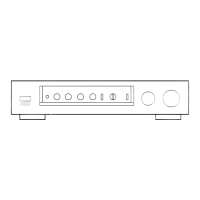
The following block diagrams show the amplifier and power supply circuits.
BLOCK DIAGRAMS
Power Supply Block Diagram
IN
YDA133
SP OUT
YDA134
YDA134
0
+B
-B
L
C
Input amp
Active power
control
Output current information
Analog
feedback
Cross
feedback
2.8 MHz
clock input
Constant-gain
PLL
modulator circuit
Real-time
protection
Real-time
protection
Protection
/mute
AC IN
88kHz
2.8MHz
(amp)
OSC
88kHz
100V(on)
200V(off)
+B
-B
OV
+
-
0V
2.8MHz
(amp)
Line filter
Choke
Inrush
protection
circuit
Sub-
transformer
Protection circuit
Microcomputer
Isolator
Right-channel power supply
Driver
Driver
For op-amps
and LSI
Magnetically
-coupled
rectifier circuit
External interface
Amplifier Block Diagram
01-MX-D1_GB_E.fm Page 6 Wednesday, October 22, 2003 2:05 PM