Pin
No.
Function
Name
I/O
(*1)
Detail of Function
1 GPIO5 Is/O General-Purpose I/O pins
2 GPIO4 Is/O These I/O pin are assigned to the digital audio pins (WCK/BCK/SDIx/SDOx)
3 GPIO3 Is/O with AIFMD[3:0] register (5V tolerant)
4 DVSS – GND
5 GPIO2 Is General-Purpose I/O pins
6 GPIO1 Is These I/O pin are assigned to the digital audio pins (WCK/BCK/SDIx/SDOx)
7 GPIO0 Is with AIFMD[3:0] register (5V tolerant)
8 PLLVDD – PLL power supply ranging from 1.65V to 1.95V (*4)
9 IC_N Is Hardware reset pin (5V tolerant)
10 PLLVSS – PLL GND (*2)
11 PLLVSS –
12 XIN I Clock input pin
Connect a 22.5792MHz or 24.576MHz crystal resonator as shown in the example below (*3, 4)
When a crystal resonator is not used, feed a clock of 22.5792MHz or 24.576MHz to XIN pin
(Change the input clock frequency only when IC_N is at “L” level)
13 XOUT O Clock output pin
Connect the external circuit as shown in the example below (*3)
When an external clock is directly fed to XIN pin without a crystal resonator, leave this pin open
Use this pin only for clock generation
14 IOVDD – Control interface power supply ranging from 3.0V to 3.6V
15 SCL Is I2C control bus clock input pin (not 5V tolerant)
16 SDA Is/Od I2C control bus data I/O pin (not 5V tolerant)
17 OPEN – Leave this pin open (*5)
18 DVSS – GND
19 IRQ_N Od Interrupt request output pin to the host controller (Interrupt request generating from DSP block)
20 DVDD18 – Core power supply ranging from 1.65V to 1.95V
21 GPIO11 Is/O General-Purpose I/O pins
These I/O pin are assigned to the digital audio pins (WCK/BCK/SDIx/SDOx)
with AIFMD[3:0] register (5V tolerant)
22 TESTb Is Test pin
Connect this pin to the GND
23 DVSS – GND
24 OPEN – Leave this pin open (*5)
25 DVSS – GND
26 GPIO10 Is/O General-Purpose I/O pins
27 GPIO9 Is/O These I/O pin are assigned to the digital audio pins (WCK/BCK/SDIx/SDOx)
28 GPIO8 Is/O with AIFMD[3:0] register (5V tolerant)
29 IOVDD – Control interface power supply ranging from 3.0V to 3.6V
30 GPIO7 Is/O General-Purpose I/O pins
These I/O pin are assigned to the digital audio pins (WCK/BCK/SDIx/SDOx)
with AIFMD[3:0] register (5V tolerant)
31 DVDD18 – Core power supply ranging from 1.65V to 1.95V
32 GPIO6 Is/O General-Purpose I/O pins
These I/O pin are assigned to the digital audio pins (WCK/BCK/SDIx/SDOx)
with AIFMD[3:0] register (5V tolerant)
*1 I/O symbols
I: Input pin Is: Schmitt trigger input pin O: Output pin Od: Open-drain output pin Ot: Tri-state output pin I/O: I/O pin
Is/Od: I/O pin (schmitt trigger input pin, Open-drain output pin) –: Power supply pin, GND pin
*2 PLLVDD and DVDD18 should be same voltage because they are internally connected each other.
PLLVSS and DVSS pins are also internally connected as well.
*3 XIN pin input frequency
24.576MHz clock should be fed to XIN pin if MDSP2 firmware stored in the on-chip ROM is used.
*4 The figure below shows an example of connecting a crystal resonator.
* Select appropriate resistor and capacitor values according to the resonator’s specification.
*5 OPEN pins must not be connected each other.
Xin Xout
22.5792MHz
24.576MHz
106
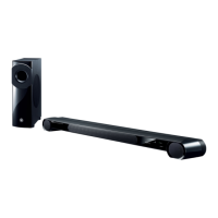
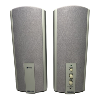
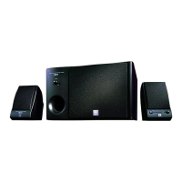
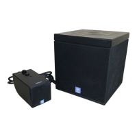
YSP-CU4300/YSP-CU3300/NS-WSW160
YSP-CU4300/YSP-CU3300/
NS-WSW160