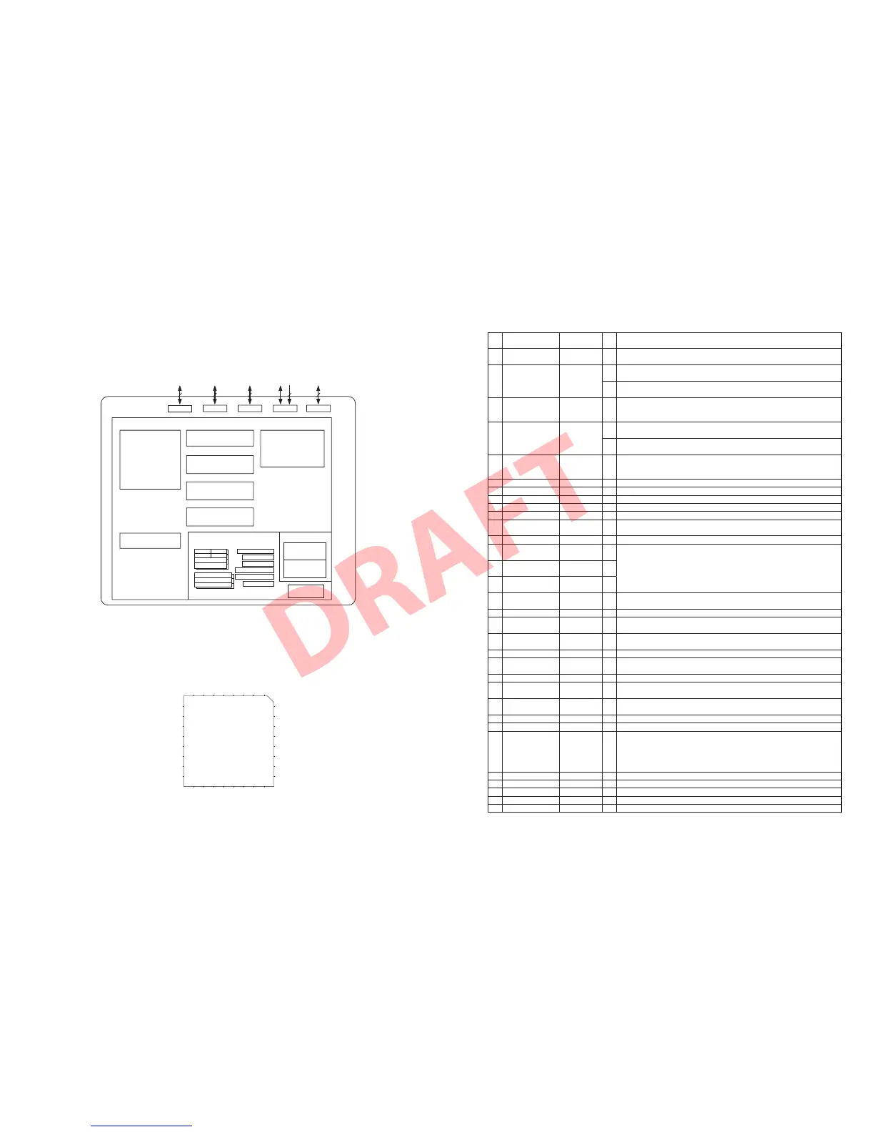
IC501: R5F21266SNFP (DSP P.C.B.)
Single chip 16-bit microprocessor
* No replacement part available. /
サービス部品供給なし
R0H
Timers
Port P0
886132
Port P1 Port P3 Port P4 Port P5
A/D converter
(10 bits x 12 channels)
System clock
generation circuit
XIN-XOUT
High-speed on-chip oscillator
Low-speed on-chip oscillator
XCIN-XCOUT
(3)
UART or
clock synchronous serial I/O
(8 bits x 2 channels)
I
2
C bus interface or clock synchronous
serial I/O with chip select
(8 bits x 1 channel)
LIN module
(1 channel)
Watchdog timer
(15 bits)
Timer RA (8 bits)
Timer RB (8 bits)
Timer RC
(16 bits x 1 channel)
Timer RE (8 bits)
R8C microprocessor core Memory
I/O ports
Peripheral functions
R0L
R1H R1L
R2
SB
INTB
PC
USP
ISP
FLG
ROM
(1)
RAM
(2)
Multiplier
NOTES:
1. ROM size varies with MCU type.
2. RAM size varies with MCU type.
3. CXIN, XCOUT can be used only for N or D version.
R3
A0
A1
FB
R5F21266SNFP
IC501
MODE
VCC/AVCC
XIN
VSS/AVSS
XOUT
N_RESET
TXD1
SCL
8
7
6
5
4
3
2
1
17
18
19
20
21
22
23
24
TXD0
GSEL1
GSEL2
VREF
(KEY)
SEL0
SEL1
SDA
9
10
11
12
13
14
15
16
RXD1
Fschange
CHG_I
N_RES_AW
P5_4
P5_3
P1_6
RXD0
N_RES_952
N_MUTE
STATUS_LED
EM_OFF
P-CON
P0_5
PROT
VOL_DET
32
31
30
29
28
27
26
25
Pin
No.
Port Name
Function
Name
I/O Detail of Function
1 P3_5/SCL/SSCK/ MODE I Connect this pin to VCC via a resistor
(TRCIOD)
2 P3_7/TRAO/SSO/ VCC/AVCC I Apply 2.2 to 5.5 V (J, K version are 2.7 to 5.5 V) to the VCC pin
RXD1/(TXD1) Apply 0 V to the VSS pin
I Power supply for the A/D converter
Connect a capacitor between AVCC and AVSS
3 RESET XIN I These pins are provided for XIN clock generation circuit I/O
Connect a ceramic resonator or a crystal oscillator between the XIN and XOUT pins
To use an external clock, input it to the XIN pin and leave the XOUT pin open
4 XOUT/XCOUT/ VSS/AVSS I Apply 2.2 to 5.5 V (J, K version are 2.7 to 5.5 V) to the VCC pin
P4_7 Apply 0 V to the VSS pin
I Power supply for the A/D converter
Connect a capacitor between AVCC and AVSS
5 VSS/AVSS XOUT O These pins are provided for XIN clock generation circuit I/O
Connect a ceramic resonator or a crystal oscillator between the XIN and XOUT pins
To use an external clock, input it to the XIN pin and leave the XOUT pin open
6 XIN/XCIN/P4_6 N_RESET I Input “L” on this pin resets the MCU
7 VCC/AVCC TXD1 O Transmit data output pin
8 MODE SCL I/O Clock I/O pin
9 P4_5/INT0/(RXD1) RXD1 I Receive data input pin
10 P1_7/TRAIO/INT1 Fschange I/O
11 P3_6/(TXD1)/ CHG_I I/O
(RXD1)/(INT1)
12 P3_1/TRBO N_RES_AW I/O
13 P5_4/TRCIOD P5_4 I/O CMOS I/O ports
Each port has an I/O select direction register,
14 P5_3/TRCIOC P5_3 I/O allowing each pin in the port to be directed for input or output individually
Any port set to input can be set to use a pull-up resistor or not by a program
15 P1_6/CLK0/(SSI) P1_6 I/O P1_0 to P1_7 also function as L
16 P1_5/RXD0/ RXD0 I Receive data input pin
(TRAIO)/(INT1)
17 P1_4/TXD0 TXD0 O Transmit data output pin
18 P1_3/KI3/AN11/ GSEL1 I/O
(TRBO)
19 P1_2/KI2/AN10/ GSEL2 I/O
TRCIOB
20 VREF/P4_2 VREF I Reference voltage input pin to A/D converter
21 P1_1/KI1/AN9/ (KEY) I/O
TRCIOA/TRCTRG
22 P1_0/KI0/AN8 SEL0 I/O
23 P3_3/INT3/SSI/ SEL1 I/O
TRCCLK
24 P3_4/SDA/SCS/ SDA I/O Data I/O pin
(TRCIOC)
25 P0_7/AN0 VOL_DET I/O
26 P0_6/AN1 PROT I/O
27 P0_5/AN2/CLK1 P0_5 I/O CMOS I/O ports
Each port has an I/O select direction register,
allowing each pin in the port to be directed for input or output individually
Any port set to input can be set to use a pull-up resistor or not by a program
P1_0 to P1_7 also function as L
28 P0_4/AN3/TREO P-CON I/O
29 P0_3/AN4 EM_OFF I/O
30 P0_2/AN5 STATUS_LED I/O
31 P0_1/AN6 N_MUTE I/O
32 P0_0/AN7/(TXD1) N_RES_952 I/O
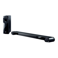
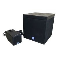
YSP-CU4300/YSP-CU3300/NS-WSW160
107