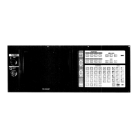
17.3 EXPLANATION OF GENERAL-PURPOSE
1/0 SIGNALS
17.3.1 l/O PORTS
(1) The YASNAC J50 contains the programmable controller system
(PC). External signals can deallocated toits I/O ports freely
when the machine manufacturer designs a built-in PC. For
details, refer to Instruction Manual for YASNAC J50 PC System
(SIE-C843-12.1).
CNC UNIT
17.3.2 1/0 CIRCUITS OF 1/0 PORTS
17.3.2.1
1/0 MODULE TYPE JANCD-FC810/FC860
(1) Input Circuits
OV common and 24 V common can be set by an external device
for the input circuit.
Internal power supply and external power supply can be used
for 24 V power supply.
(a) When the internal power
supply is used.
T-T
PANEL
NC
I/o
)
MACHINE
MAIN
*lloo -
SEOUENCER
PROCESSING
#1200 -
#looo-
<
#1300 -
GNERAL-
PURPOSE
l,:HNE &“)+E
1/0
#1116 -
I
I
y
lW-J
PORTSET AOORESSSET
Fig. 17,36 System Configuration
(2)
The general-purpose 1/0 ports are mounted on the 1/0 module
types JANCD-FC8 10, FC860, FC861 and on the SP50 board of
the CNC operator’s panel.
The numbers of 1/0 points of these modules are shown in Table
17.1.
Table 17.1 Numbers of 1/0 Points of Modules
Module Type Input
output
JANCD-
Points
Remarks
Points
Fc810/Fc860 112
96
4
FCS61
64
56
I
For machine panels
SP50-1 64 32
I 1
SP50-2 64
56
Notes :
1. YASNAC J50 needs one 1/0 board incorporated in a CNC operator’s panel
(SP50-1 or SP50-2). Therefore, up to 3 board (max. inputs: 512 points, max.
outputs: 344 points) can be connected when only FC 810/FC860 is added. Up to
7 boards (max. inputs: 512 points, max. outputs: 448 points) can be connected,
2. Each module can be used together with the other, However, an 1/0 mea number
must not be overlapped. (Refer to Appendix 2.) If any 1/0 area number is
overlapped, alarm No. 374 occurs m status chunges to the input disabled status.
3. In order to muke it possible to add more modules, it is necessary for each 1/0
module to terminate the fhal board,
(3) Address Setting
The relationship between the address and connectors is
indicated in Table 18.1. (This table applies to port 1. If a
different port is used, address changes are required.
Table 17.2 Address and Connector
#I 002
#loo3
#loo4
I CN5
#1 005
#1006
v
lrIput Output (JANCD- ,:;::::, ) (JANCD- ::8M )
#I 007
CN6 1
#l 008
:~ ~ COM41
.
#1 009
—
CN5
COM42
#lolo
—
#lo] 1
—
:: I COM20
#1012 CN3
COM2 1
#1013
—
CN2
COM 10
#l loo CN4
CN1
#llol CN4
CN 1
#llo2 CN5
CN 1
#1103 CN5
CN 1
#1 104 ICN6]
CN1
#1 105 ICN61
CN2
#1 I06 icN6j
i
CN3
#1107 —
CN3
#1108 —
CN6
;.neral. purpose I/o
:JANCD-FC861)
::; ~ COMOO
CN 1
COMOI
:~ ~ COM02
CN2
COM03
:~ 3 COM04
CN
1
CNI
CN2
CN2
CN3
CN3
CN3
1N64JOUT56
OV Common
I
t----l
ox
L-J
+24 V Common
Fig. 17,37 Internal Input Circuits
(b) When the external power supply is used.
I
024
OV Common
l-.----+--
I
1+
I
0,,
,
L.d
+24 V Common
Fig. 17.38 External Input Circuits
Note :
“Common” in the input circuit (for example, COM1O, COM20, COM21...total
9) cuu be either “+24
V common”’or “O V common” for every 8 or 16 input
points as mentioned in Par. 17.3 1/0 signal interface and can be selected
freely. Set by wiring on the cable side.
85
 Loading...