Principles of Operation 85
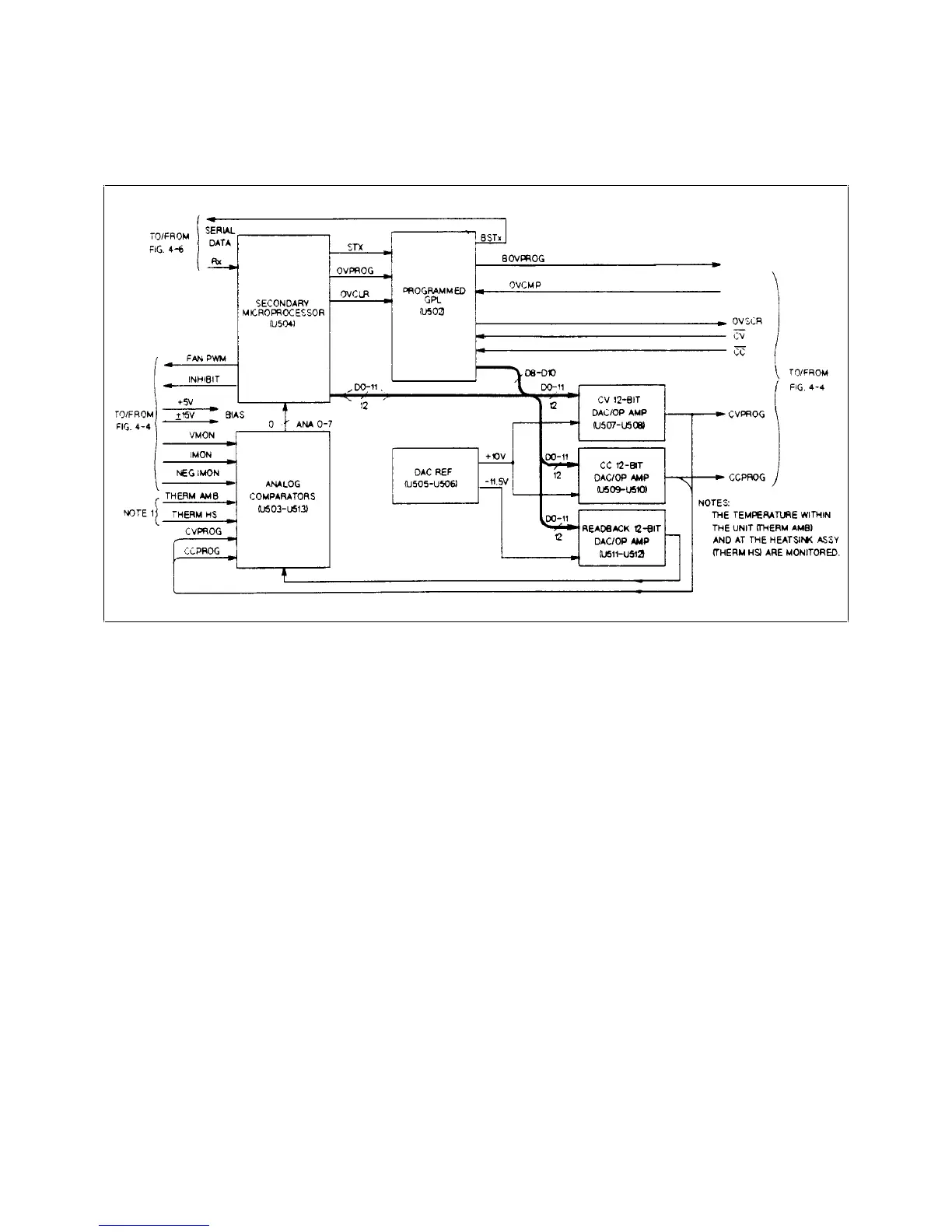
The readback DAC circuit is controlled by the microprocessor to successively approximate the value of each signal
monitored to twelve-bit resolution. The CVPROG and CCPROG signals are used during the self test to check operation of
the DAC/Op amplifier circuits.
Figure 4-3. Secondary Interface, Simplified Block Diagram
The microprocessor produces the FAN PWM signal, whose pulse width is varied depending upon the ambient temperature.
The FAN PWM signal is applied to the fan speed control circuit in order to speed up the fan as temperature increases, and
to slow the fan speed down as temperature decreases.
The INHIBIT signal is generated by the microprocessor to hold the supply’s output off during turn-on and when the supply
OVs. The INHIBIT signal is sent to the output stage bias/shutdown circuit in order to shutdown the bias voltage to the
output stages, and to keep the supply output off.
The microprocessor produces the OVPROG signal, which is also a pulse-width modulated signal that represents the
programmed over voltage protection level. The OVPROG signal is sent to the OV monitor circuit, which compares the
actual output voltage level with the OVPROG signal. When the output voltage exceeds the OVPROG signal level, the OV
monitor circuit produces a low-level OVCMP* signal. With OVCMP* low, the GAL produces a high-level OVSCR signal
which is sent to the SCR control and to the output stage bias/shutdown circuits. The high-level OVSCR signal causes the
following actions to occur:
• The SCR fires, shorting the supply’s output.
• The GATED ±15 V bias for the output regulators on the tunnel boards is shut down, turning off the output.
• The GAL notifies the secondary microprocessor of the OV condition (OVSCR is high) on data line eleven, in order to
display a status update.
• The microprocessor clears the OVSCR signal when it generates the OVCLR signal (output protection clear command is
executed).
 Loading...