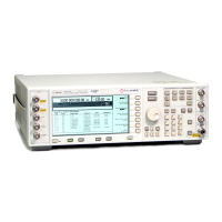
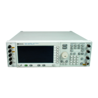
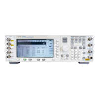
ESG Family Signal Generators Front and Rear Panel
Rear Panel Overview
User’s Guide 3-15
12. PATTERN TRIG IN Connector
This input can accept either a TTL/CMOS low to TTL/CMOS high or TTL/CMOS high to
TTL/CMOS low edge trigger. The minimum trigger input pulse width, high or low, is
100 ns. The damage levels are > +8 and <
−
4 V. This female BNC connector is provided
only on instruments with Option UN8 or UND. If you configure your instrument with
Option 1EM, this input is changed from a BNC to an SMB connector.
With Option UN8 turned on, the input to the PATTERN TRIG IN connector is used to
trigger the internal digital modulation pattern generator to start a single pattern output or
to stop and re-synchronize a pattern that is being continuously output. The trigger edge is
latched and then sampled by the falling edge of the internal data bit clock to synchronize
the trigger with the data bit clock timing. The minimum delay from the trigger edge to the
first bit of the frame is 1.5 to 2.5 bit clock periods. For more information on pattern
triggering, refer to the “Operation” chapters in the user’s and programming guides.
With Option UND turned on, this connector is the source for the external trigger for all of
the ARB waveform generator triggers. With Option 201 this connector is used for system
reset trigger input.
13. BURST GATE IN Connector
The BURST GATE IN connector accepts a TTL or CMOS signal for gating burst power in
digital modulation applications. The burst gating is used when you are externally
supplying data and clock information. The input signal must be synchronized with the
external data input that will be output during the burst. The burst power envelope and
modulated data are internally delayed and re-synchronized. The input signal must be
CMOS high for normal burst RF power or CW RF output power and CMOS low for RF off.
The leading edges must be synchronous with the DATA CLOCK rising edges. The signal
level must be valid on the DATA CLOCK falling edge. The damage levels are > +8 and
<
−
4 V. This female BNC connector is provided only on instruments with Option UND or
UN8. If you configure your instrument with Option 1EM, this output is changed from a
BNC to an SMB connector. With Option 201 this connector is used for even second
synchronization input.
14. COHERENT CARRIER OUT Connector
This connector outputs RF that is not modulated with AM, pulse, or I/Q modulation, but is
modulated with FM or ΦM. The output power is nominally 0 dBm ±5 dB. The output
frequency range is from 249.99900001 MHz to the maximum specified frequency of your
signal generator. If the RF output frequency is below this range, the COHERENT
CARRIER OUT signal will have the following frequency: Frequency of coherent
carrier = (1E9 − Frequency of RF output) in Hz. The damage levels are 20 Vdc and 13 dBm
reverse RF power. This SMA connector is present only on ESG-D and ESG-DP Series
Signal Generators.
15. ALT PWR IN Connector
This BNC connector accepts a CMOS signal for synchronization of external data and
alternate power signal timing. Damage levels are > +8 V and < −4 V. This connector is
active only with Options UNA or 201. With Option 201 this connector is used for Long
Code State Latch strobe input.
 Loading...


