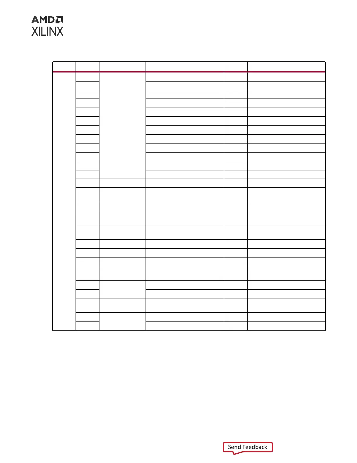
Table 7: MIO Peripheral Mapping (cont'd)
Bank MIO # Device Signal I/O Notes
502 0 GEM0 LPD_MIO0_GEM_TX_CLK O GEM_TX_CLK
1 LPD_MIO1_GEM_TX_D0 I/O GEM_TX_D0
2 LPD_MIO2_GEM_TX_D1 I/O GEM_TX_D1
3 LPD_MIO3_GEM_TX_D2 I/O GEM_TX_D2
4 LPD_MIO4_GEM_TX_D3 I/O GEM_TX_D3
5 LPD_MIO5_GEM_TX_CTL I/O GEM_TX_CTL
6 LPD_MIO6_GEM_RX_CLK I GEM_RX_CLK
7 LPD_MIO7_GEM_RX_D0 I/O GEM_RX_D0
8 LPD_MIO8_GEM_RX_D1 I/O GEM_RX_D1
9 LPD_MIO9_GEM_RX_D2 I/O GEM_RX_D2
10 LPD_MIO10_GEM_RX_D3 I/O GEM_RX_D3
11 LPD_MIO11_GEM_RX_CTL I/O GEM_RX_CTL
12
13 Regulator Enable
GPIO
VCC_SOC_EN_LS O VCC_SOC Power Enable
14
15 Regulator Enable
GPIO
VCC_PSFP_EN_LS O VCC_PSFP Power Enable
16 Regulator Enable
GPIO
VCC1V1_LP4_AUX_EN_LS O VCC1V1, Aux Power Enable
17
18
19
20 Regulator Enable
GPIO
VCC_PL_EN_LS O VCC PL Power Enable
21 FAN MIO21_FAN_PWM_VERSAL O Versal ACAP Fan PWM
22 MIO22_FAN_TACH_VERSAL I Versal ACAP Fan Tach
23 Regulator Enable
GPIO
VADJ_FMC_EN_LS O VADJ_FMC Enable
24 MDIO LPD_MIO24_GEM_MDC O GEM MD Clock
25 LPD_MIO24_GEM_MDIO I/O GEM MD I/O
PMC MIO[0–12] Bank 500: QSPI U11, U12
[Figure 3, callout 36]
The VPK180 evaluaon board uses two Micron MT25QU01GBBB8E12-0SIT 4-bit serial
peripheral interface (quad SPI) ash devices. These 1 Gb NOR ash devices are organized in a
dual parallel conguraon and can be used as onboard boot, as well as non-volale storage
memory. When used as a boot source, it is selectable from SW1. See Switches for more
informaon.
Chapter 3: Board Component Descriptions
UG1582 (v1.0) February 21, 2023 www.xilinx.com
VPK180 Board User Guide 32