ADE9000 Technical Reference Manual UG-1098
Rev. 0 | Page 3 of 86
ANALOG-TO-DIGITAL CONVERTER (ADC)
OVERVIEW
The ADE9000 incorporates seven independent, second-order,
Σ-Δ ADCs that sample simultaneously. Each ADC is 24 bits and
supports fully differential and pseudo differential inputs, which
can go above and below ground. The ADE9000 includes a low
noise, low drift, internal band gap reference. Set the EXT_REF
bit in the CONFIG1 register if using an external voltage
reference. Each ADC contains a programmable gain amplifier
which allows a gain of 1, 2, or 4.
ANALOG INPUT CONFIGURATION
There is no internal buffering; the impedance of the ADE9000
depends on the programmable gain selected.
Fully Differential Inputs
The input signals on the IAP, IAN, IBP, IBN, ICP, ICN, VAP,
VAN, VBP, VBN, VCP, and VCN pins must not exceed 0.6 V.
The differential full-scale input range of the ADCs is ±1 V peak
(0.707 V rms).
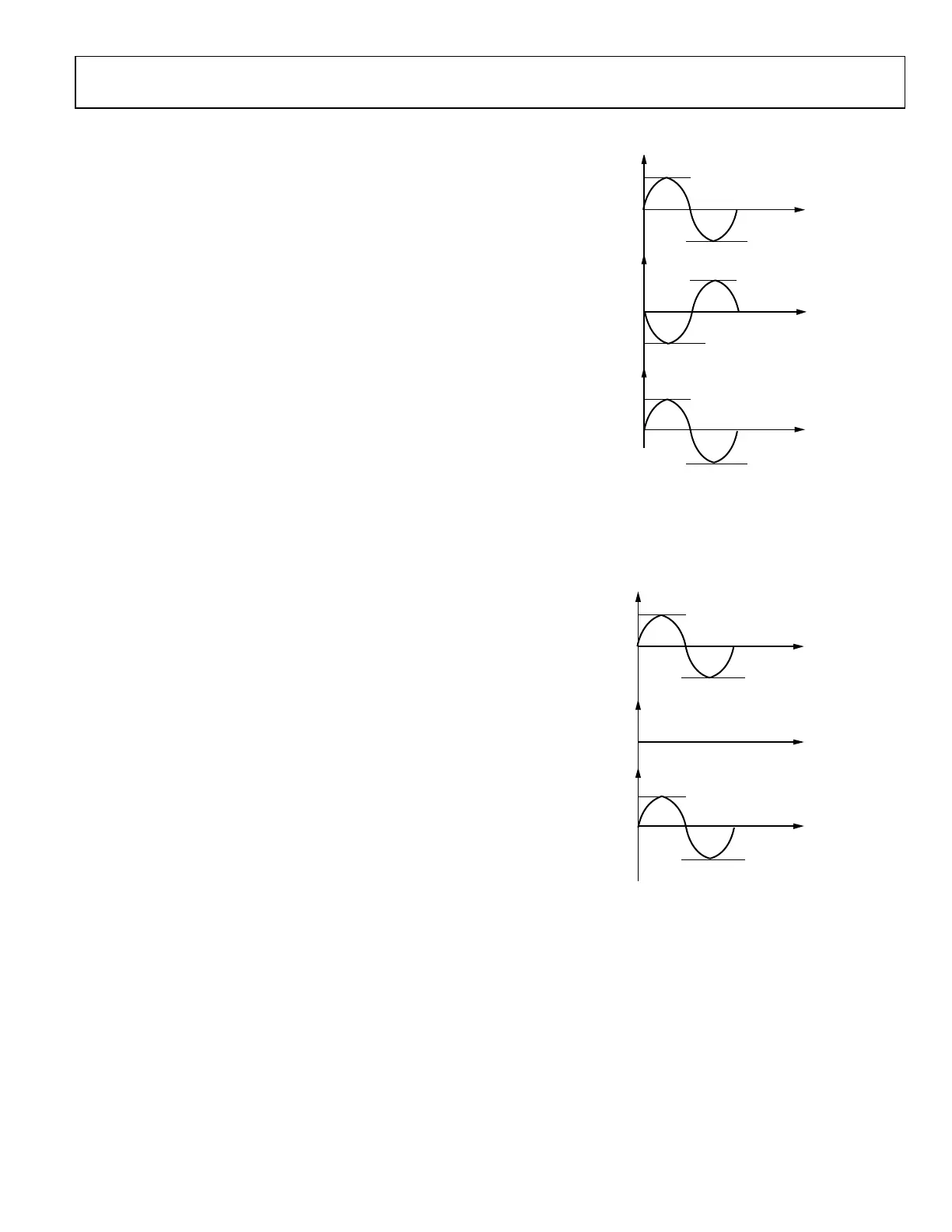
Figure 2 and Figure 3 show two common types of input signals
for an energy monitoring application. Figure 2 shows the
maximum input allowed with differential antiphase signals.
A current transformer with center tapped burden resistor
generates differential, antiphase signals. Figure 3 shows the
maximum input signal with pseudo differential signals, similar
to those obtained when sensing the mains voltage signal through
a resistive divider or using a Rogowski coil current sensor.
The following conditions must be met for the input signals with
gain = 1:
• |IAP, IAN, IBP, IBN, ICP,ICN, VAP, VAN, VBP, VBN, VCP,
and VCN| ≤ +0.6 V peak
• |IxP − IxN| ≤ +1 V peak, |VxP − VxN| ≤ +1 V peak
Each ADC contains a programmable gain amplifier which allows
a gain of 1, 2, or 4. The ADC produces full-scale output codes
with an input of ±1 V. With a gain of 1, this full-scale output
corresponds to a differential antiphase input of 0.707 V rms,
as shown in Figure 2. At a gain of 2, full-scale output codes are
produced with an input of 0.353 V rms, as shown in Figure 3. At
gain of 4, full-scale output codes are generated with a 0.1765 V rms
input signal. Note that the voltages on the xP and xN pins must
be within ±0.6 V, as specified in the data sheet.
Write the x_GAIN bits in the PGA_GAIN register to configure
the gain for each channel.
+0.1V
0
+0.6V
–0.4V
0x0471 44AD =
NOTES
1. x_PCF IS THE INST
ANT
ANEOUS
WA
VEFORM OBT
AINED
AFTER GAIN
AND PHASE COMPENS
A
TION.
+74,532,013
0xFB8E BB53 =
–74,532,013
CHANNE
L (x_PCF)
WA
VEFORM
D
ATA
RANGE WITH x_GAIN = 1
xP
INPUT PIN
xM INPUT PIN
+0.1V
+0.6V
–0.4V
15523-002
Figure 2. Maximum Input Signal with Differential Antiphase Input with
Common Mode Voltage = 0.1 V, Gain = 1
+0.1V
0
+0.6V
–0.4V
+0.1V
0x0471 44AD =
+74,532,013
0xFB8E BB53 =
–74,532,013
CHANNEL (x_PCF) WAVEFORM
DATA RANGE WITH x_GAIN = 2
xP INPUT PIN
xM INPUT PIN
NOTES
1. x_PCF IS THE INSTANTANEOUS WAVEFORM OBTAINED
AFTER GAIN AND PHASE COMPENSATION.
15523-003
Figure 3. Maximum Input Signal with Pseudo Differential Input with
Common Mode Voltage = 0.1 V, Gain = 2
 Loading...