ADE9000 Technical Reference Manual UG-1098
Rev. 0 | Page 7 of 86
POWER MANAGEMENT
POWER MODES
The ADE9000 offers two operating modes, PSM0 and PSM3.
The entry into the power modes is controlled by the PM1 and
PM0 pins. These pins are checked continuously to determine
which operating mode to enter. If it is desired to place the
ADE9000 into a low power reset state, PSM3 can be used.
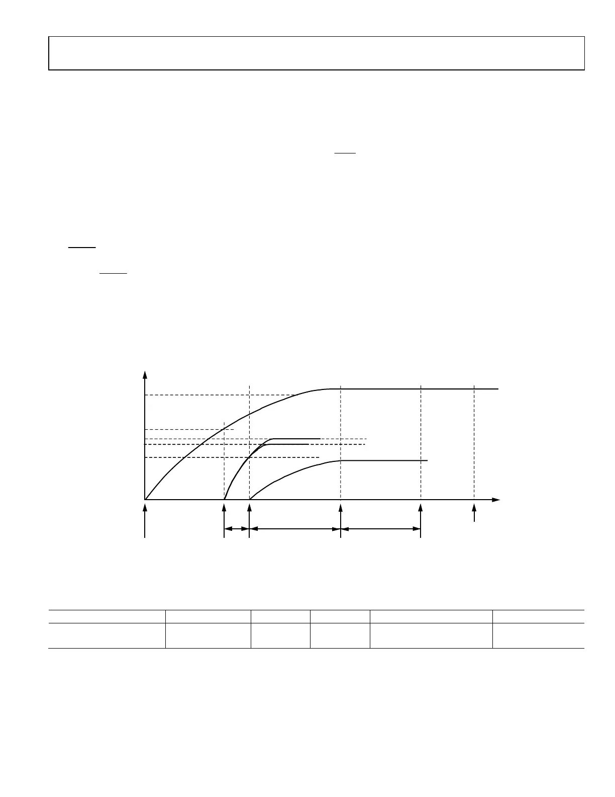
POWER-ON SEQUENCE
After power is applied to the VDD pin of the ADE9000 IC, the
device checks the state of the PM0 and PM1 pins to check the
power supply mode (see the Power Modes section for more
information). If in PSM0 mode (PM1 and PM0 = 00 or 01) and
the
RESET
pin is high, the AVDD and DVDD low dropout
regulators (LDOs) are turned on when VDD reaches 2.4 V to
2.6 V. If the
RESET
pin is low, the AVDD and DVDD LDOs are
not turned on. Note that there is a clamp that limits the current
used to charge the AVDD and DVDD LDOs to 17 mA per LDO.
When AVDD and DVDD are both above 1.3 V to 1.5 V and
VDD is above 2.4 V to 2.6 V, a 20 ms timer is started to allow
additional time for the supplies to come to their normal
potentials (VDD between 2.97 V and 3.6 V, AVDD at 1.9 V, and
DVDD at 1.7 V). After this timer has elapsed, the crystal
oscillator is started.
The RSTDONE interrupt is triggered 26 ms later, bringing the
IRQ1
pin low and setting the RSTDONE bit in the STATUS1
register. The RSTDONE bit being set indicates to the user that
the ADE9000 has finished its power-up sequence. The user can
now configure the IC via the serial peripheral interface (SPI).
After configuring the device, write the RUN register to start the
DSP so that it starts making measurements. Note that registers
from Address 0x000 through Address 0x0FF and Address 0x400
through Address 0x5FF are restored to their default values
during power-on. Registers from Address 0x200 through
Address 0x3FF are cleared within 500 μs from when the RUN
register value changes from 0x0000 to 0x0001. Also note that
the waveform buffer, Address 0x800 through Address 0xFFF, is
not cleared after reset.
In PSM3 mode, the AVDD and DVDD LDOs are not turned
on. The RSTDONE interrupt does not occur, and the SPI port is
not available
HOST CONFIGURES
IC VIA SPI AND THEN
WRITES RUN
REGISTER TO START
MEASUREMENTS
20ms0.5ms
0
VOLTAGE (V)
2.4V TO 2.6V
2.97V TO 3.63V
VDD
DVDD
~26ms
1.7V
AVDD1.9V
VREF
ADE9000
1.3 TO 1.5V
RSTDONE
INTERRUPT
TRIGGERED
CRYSTAL
OSCILLATOR
STARTS
POR TIMER
TURNED ON
AVDD, DVDD
LDO TURNED
ON
POWER APPLIED
TO IC
IN PSM0
15523-009
Figure 9. ADE9000 Power-On Sequence for PSM0
Table 4. Power Modes (PSM0 and PSM3)
PSMx Power Mode Description PM1 Pin PM0 Pin Functions Available SPI Available?
PSM0 Normal mode 0 0 or 1 All functions Yes
PSM3 Idle 1 1 None No