EVAL-AD9081/EVAL-AD9082/EVAL-AD9986/EVAL-AD9988 User Guide UG-1829
Rev. 0 | Page 11 of 26
EVALUATION BOARD HARDWARE SETUP
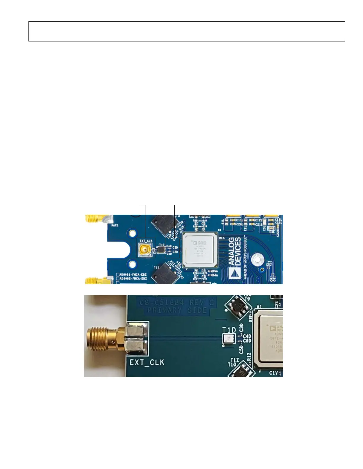
DETERMINE THE CLOCK SOURCE
Determine whether the AD9081-FMCA-EBZ, AD9082-FMCA-
EBZ, AD9986-FMCB-EBZ, or AD9988-FMCB-EBZ is set to the
external clock or on-board HMC7044 clock by checking the C3D,
C4D, C5D, and C6D capacitors on the evaluation board chosen. By
default, the HMC7044 clock is enabled (C3D and C5D are
placed on the evaluation board, and C4D and C6D are do not
insert (DNI)). If using a direct external clock, remove the C3D
and C5D capacitors and place the C4D and C6D capacitors on the
evaluation board. The capacitors are 0.1 μF, size 0201 (imperial) or
size 0603 (metric). For additional details, see Figure 18 and
Figure 19.
DEFAULT CLOCKING SCHEME FOR AD9081-FMCA-
EBZ, AD9082-FMCA-EBZ, AD9986-FMCB-EBZ, OR
AD9988-FMCB-EBZ
The default clocking scheme for these evaluation boards uses
the on-chip phase-locked loop (PLL) within the AD9081, AD9082,
AD9986, or AD9988. The HMC7044 provides the reference
input to the chip. The evaluation board provides all the necessary
clocks for conducting a quick evaluation of the device, including
the auxiliary clocks needed by the FPGA in the ADS9-V2EBZ
board to set up the JESD204B or JESD204C link. The clocking
scheme is shown in Figure 20. As shown in Table 1, the reference
frequencies used by the two boards (AD908x-FMCA-EBZ or
AD998x-FMCB-EBZ) are different. Therefore, each board only
supports the integer multiples of the crystal oscillator that are
on the evaluation board. The plugin only supports the integer
multiples of the crystal oscillator that are installed on the
evaluation board. If a different clock frequency is required for
evaluation, the user must modify the evaluation board to accept
an external clock by following the instructions previously listed.
This modification also necessitates an additional clock source
for the ADS9-V2EBZ. Refer to Figure 30 for additional details
on the instrument setup.
DIRECT EXTERNAL CLOCK INPUT
(SMP-F)
• PLACE C4D AND C6D FOR DIRECT EXTERNAL CLOCK INPU
• C3D AND C5D PLACED BY DEFAULT
24165-014
Figure 18. Capacitor Position for Direct External vs. On-Board HMC7044 Clocking (Showing the AD908x-FMCA-EBZ)
24165-218
Figure 19. Capacitor Position for Direct External vs. On-Board HMC7044 Clocking (Showing the AD998x-FMCB-EBZ Evaluation Board)