EVAL-AD9081/EVAL-AD9082/EVAL-AD9986/EVAL-AD9988 User Guide UG-1829
Rev. 0 | Page 13 of 26
USING THE AD9081, AD9082, AD9986, OR AD9988 BOARD VIEW
The board view allows the user to quickly set up the AD9081,
AD9082, AD9986, or AD9988 to a predetermined use case for
evaluation. The board view uses the on-board clocking solution
to manage the clocks to the AD9081, AD9082, AD9986, or
AD9988, as well as the FPGA. For more details on the clock
setup, refer to Figure 20. Figure 21 shows the hardware
connection needed when using the board view with the
AD9082-FMCA-EBZ board as an example.
USE CASES
The use cases in Table 2, Table 3, Table 4, and Table 5 are
supported for JESD204B and JESD204C modes for the AD9081-
FMCA-EBZ, AD9082-FMCA-EBZ, AD9986-FMCB-EBZ, or
AD9988-FMCB-EBZ. Tx means transmit data path, and Rx
means receive data path.
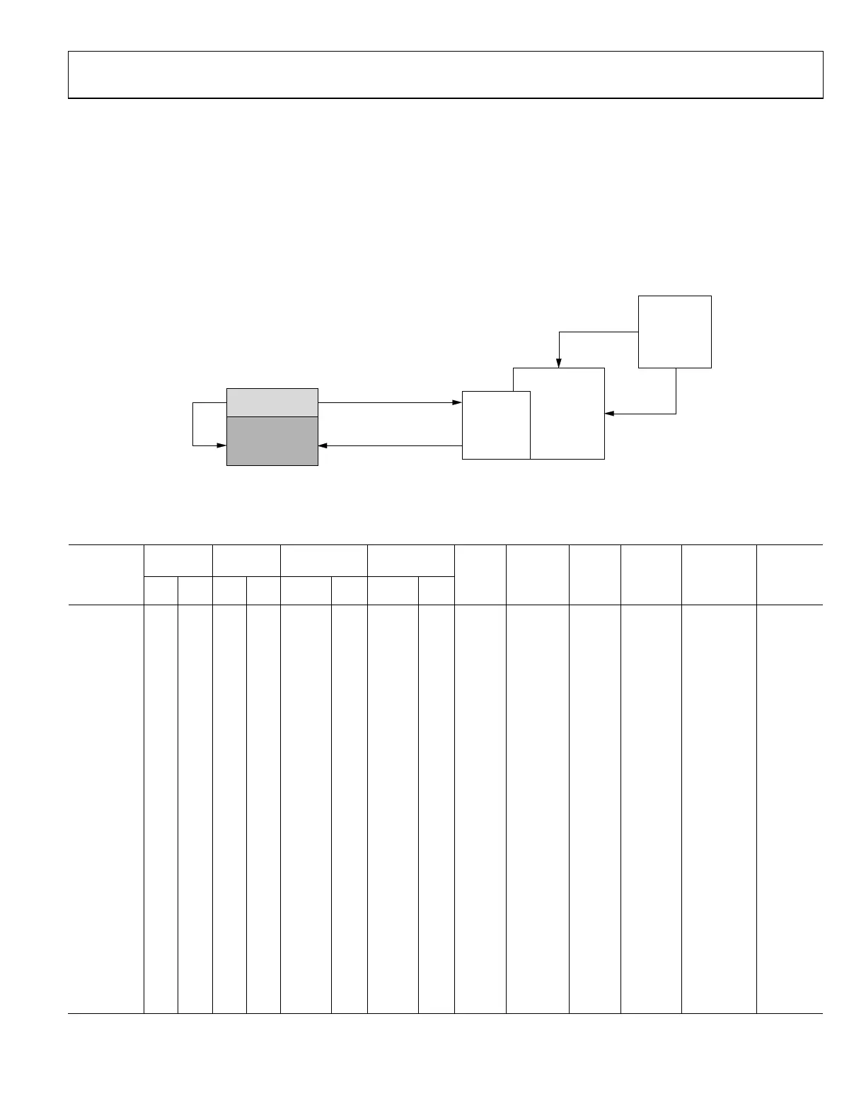
ADS9-V2EBZ
PC
USB
ETHERNET
AD9082-
FMCA-EBZ
SIGNAL
GENERATOR
ANALOG INPUT TO ADC
SPECTRUM
ANALYZER
10MHz
REFERENCE
ADC0
DAC OUTPUT
DAC0
24165-017
Figure 21. Hardware Setup for Using the Board Wizard (Note the 10 MHz Reference Connection)
In Table 2, N/A means not applicable.
Table 2. Use Cases for AD9081-FMCA-EBZ Board View (Uses 100 MHz On-Board Crystal Oscillator, All Single Link)
Description
Clock
(GHz)
JESD204x
Mode
1
Tx
Interpolation
Rx
Decimation
Tx
Data
Rate
(MSPS)
No. of Tx
Channels
Rx
Data
Rate
(MSPS)
No. of Rx
Channels
Link Line
Rate
(Gbps/lane)
JESD204x
Protocol
2
Tx Rx Tx Rx Coarse Fine Coarse Fine
12 GSPS
DAC,
1.5 GSPS
I/Q, 4 GSPS
ADC, Full
Bandwidth
12 4 15C 27C 8 1 1 1 1500 4 4000 4 24.75 C
12 GSPS
DAC,
1.5 GSPS
I/Q, 3 GSPS
ADC, Full
Bandwidth
12 3 15C 18C 8 1 1 1 1500 4 3000 4 24.75 C
6 GSPS DAC,
1.5 GSPS
I/Q, 3 GSPS
ADC, Full
Bandwidth
6 3 15C 18C 4 1 1 1 1500 4 3000 4 24.75 C
12 GSPS
DAC, 4 GSPS
ADC,
250 MSPS
I/Q
12 4 9B 10B 8 6 4 4 250 4 250 4 10 B
Dual Band
Setup,
12 GSPS
DAC, 3 GSPS
ADC,
375 MSPS
I/Q
12 3 16B 17B 8 4 2 4 375 4 375 4 15 B

 Loading...