UG-1829 EVAL-AD9081/EVAL-AD9082/EVAL-AD9986/EVAL-AD9988 User Guide
Rev. 0 | Page 22 of 26
USING THE AD9081, AD9082, AD9986, OR AD9988 CHIP VIEW
The chip view enables the user to customize the AD9081,
AD9082, AD9986, or AD9988 beyond the functions available in
the board view. Use the chip view if using a direct external
clock. The chip view provides a more customizable user
interface (UI) that directs the user through the various aspects
of the device setup. For optimal use of the chip view, provide a
direct external clock to the AD9081-FMCA-EBZ, AD9082-
FMCA-EBZ, AD9986-FMCB-EBZ, or AD9988-FMCB-EBZ.
Refer to Figure 18 and Figure 19 for information on how to
modify the board for a direct external clock. When using direct
external clock mode, the user must provide the device clock as
well as the FPGA reference clock.
SETTING UP THE AD9081 OR THE AD9082 IN FULL
BANDWIDTH MODE WITH EXTERNAL CLOCKING
Take the steps that follow to set up the AD9081 or the AD9082
in full bandwidth mode. The AD9986 or the AD9988 does not
offer full bandwidth mode. Refer to the UG-1578 to see what
options are supported by the various devices.
1. Set up the evaluation board hardware and instrumentation
as shown in Figure 30.
2. Set the clock signal generator to 6 GHz, with an amplitude
set to 5 dBm. Provide this signal to J6 of the AD9081-
FMCA-EBZ or the AD9082-FMCA-EBZ.
3. Set the reference clock signal generator to 750 MHz with
an amplitude set to 5 dBm. Provide this signal to the J1
EXT CLK connector of the ADS9-V2EBZ.
4. Set the analog input signal generator to 1.81 GHz with an
amplitude set to ~6.5 dBm. Turn the signal generator
output off for this setup.
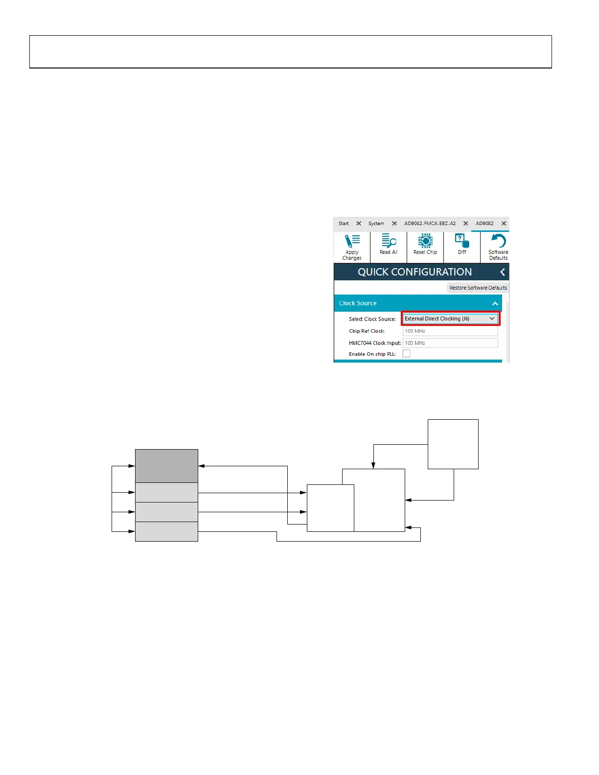
5. Open the chip view. In the QUICK CONFIGURATION
pane, select the External Direct Clocking (J6) clock source,
as shown in Figure 29.
24165-021
Figure 29. Selecting the Clock Source in Chip View
ADS9-V2EBZ
PC
USB
ETHERNET
AD9081-
FMCA-EBZ
SIGNAL
GENERATOR
CLOCK
SIGNAL
GENERATOR
ANALOG INPUT TO ADC
SIGNAL
GENERATOR
REFERENCE CLOCK
SPECTRUM
ANALYZER
10MHz
REFERENCE
ADC0
DAC OUTPUT
DAC0
24165-020
Figure 30. Hardware Setup for Using the Chip View (Note the 10 MHz Reference Connection)

 Loading...