EN-13
Theory of Operation
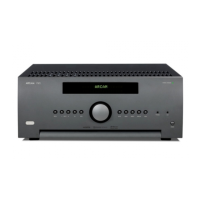
The SA30 contains three PCBs, the power amplier
PCB, Digital PCB, and front panel PCB. What follows is
an overview of each PCB as well as any signals that go
between the PCBs.
A note on standby modes
The SA30 has a number of dierent standby modes.
Modes are selected in the Network Menu.
Standby Mode Note
RS232 NET
OFF OFF Lowest power mode.
Network module disabled
no RS32 or IP control.
ON OFF Network module disabled.
RS232 control availble, no
IP control
ON ON Network module enabled.
RS232 and IP control
availble.
Power Amplier PCB - L297
The power amplier PCB has 5 main sections
• Host MCU
• Line inputs
• Volume Contrrol
• Power Amplier
• Lifter
Line Inputs
The SA30 has 5 line level inputs (4 x RCA + 1 x 3.5mm)
and a MM/MC phono stage.
The phono stage takes the low level phono signal and
ampliies to normal line level.
These inputs are then fed into the input mux IC100/104.
These single ended inputs are converted to balanced
before being fed up to the ADC.
A single ended “bypass” path is sent from here directly to
the volume control.
The balanced DAC feeds from the top PCB are converted
to singled ended here before being fed to the volume
control.
Volume control
The volume control is a digitally controlled analogue
type. The input is switched between the ADC/DAC path
and the analogue direct “bypass” path, selected by a
relay.
The output of the volume control is fed to the power
amplifer, headphone amplier and the pre-out
connectors.
Power Amplier
The power amplier is a class G design that uses a
switchable main HT rail to enable class A operation at
lower output levels and class AB for higher output levels.
Lifter
The lifter circuitry selects between two HT rails to power
the output devices in the amplier based on the output
level.
Host MCU
The host MCU, IC700 control all the functions of the
SA30 using various logic signals and control interfaces.
SPI for the front panel VFD, I2C for the DAC. SPDIF Rx and
ADC, I2C fo the network module.
It also handles the RS232 control interface.
Digital PCB - L298
The preamp PCB has four main sections
• ADC/SPDIF Rx/I2S Mux
• SPDIF reciever
• DAC
• Network module
ADC
The ADC, IC101, is an AKM5552 and is controlled by the
host MCU via I2C.
It is supplied with a 24.576Mhz master clock from the
SPDIF reciever.
The ouptut I2S audio is fed to the I2S multiplexer
IC102/103 along with the output from the SPDIF Rx.
The ADC is fed with a balanced audio input from the
main PCB.
The ADC is powered via a 5V and 3.3V rail derived from
the 9V rail generated from the power transformer.
SPDIF Reciever
The SPDIF receiver, IC100, is an AKM4113 and is
controlled by the host MCU via I2C.
The ouptut I2S audio is fed to the I2S multiplexer
IC102/103 along with the output from the ADC.
The SPDIF Rx is also used to generate the low jitter ADC
master clock.
The SPDIF Rx is powered by a 3.3V supply derivde from
the 5V digital PSU.
I2S Mux
The I2S from the SPDIF Rx and ADC is switched by
IC102/103 and is controlled by the host MCU via IC104.
The output is fed to the network module.
DAC
The ESS9038 DAC, IC204, is controlled by the host MCU
via I2C.
It is fed with I2S audio from the network module.
The DAC is powered by muliple PSUs all derived from
the 9V rail generated from the transformer.
The DAC lters and DC servos are all powered from the
+/-9V rails generated by the transformer.
The balanced output is fed to the amplier PCB via
CON2 along with the balanced ADC feeds.
Network Module
The network module MOD300 is responsible for all
network communications and processing. it includes
a 2.4/5GHz WiFi module and controls the ethernet phy,
IC301, for wired network applications.
ADC and SPDIF data is fed through the network module
to allow Dirac processing to be applied by its internal
DSP.
Front Panel - L305
The front panel PCB is connected to the main PCB via
CON900.
The VFD which is controlled by the host MCU via and
SPI interface. These signals are traslated from 3.3V to 5V
by IC901.
VFD is powered by a 5V rail from the main PCB. The grid
and electrode voltages are supplied by the transformer
via CON901.
Front panel keys are arranged to form a potential divider
with a 10k pull up on the main PCB and the MCU uses its
internal ADC to determine which key or combination of
keys has been pressed.