SWITCH EQUIVALENT OF DEVICE 9322 (I.E., H2)
AO
64H
AO
64H
ZA =
ADDR3
ZA
= 64H
A1
ADDR3
A1
ADDR3
32H
BO
32H
BO
i!B
= ADDR 2
ZB = 32H
ADDR2
B1
ADDR2
B1
16H
co
16H
co
~C
= ADDR 1
C1
ZC = 16H
ADDR1
C1
ADDR 1
SH
DO
SH
DO
D1
i!D
= ADDR 0
D1
ZD
=SH
ADDRO
ADDRO
<1>2
=HIGH
<1>2:::
LOW
rfL;
f-tI'
Figure
3-12
Address Multiplexers Equivalent Diagram
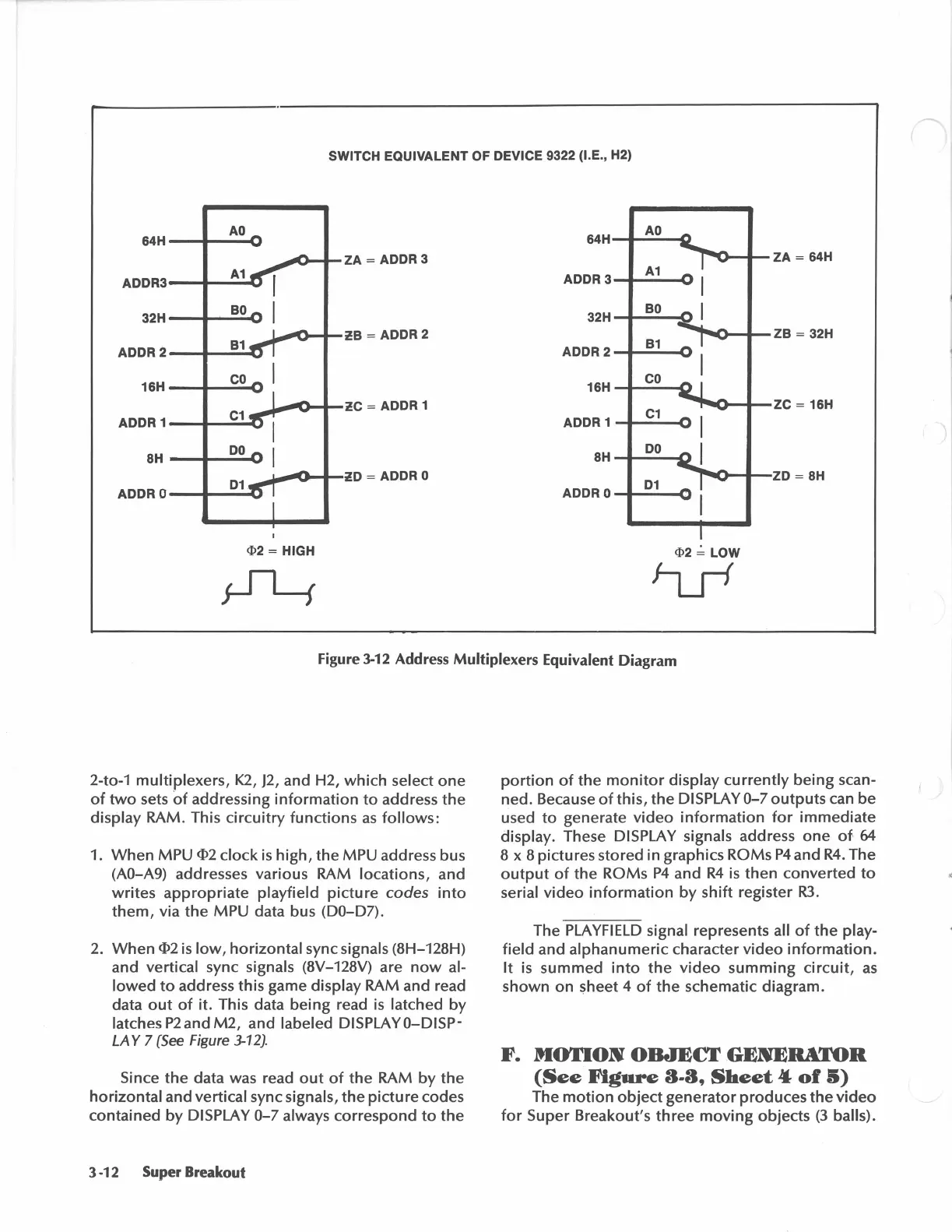
2-to-1
multiplexers,
K2,
J2,
and H2,
which
select
one
of
two
sets
of
addressing
information
to
address
the
display RAM. This
circuitry
functions
as
follows:
1.
When
MPU
<1>2
clock
is
high,
the
MPU address bus
(AO-A9) addresses various RAM
locations,
and
writes
appropriate
playfield
picture
codes
into
them,
via
the
MPU data bus (DO-D7).
2.
When
<1>2
is
low,
horizontal
sync signals (8H-128H)
and vertical sync signals
(8V-128V) are
now
al-
lowed
to
address this game display RAM and read
data
out
of
it. This data
being
read
is
latched
by
latches P2and
M2,
and labeled DISPLAYO-DISP-
LA
Y 7
(See
Figure
3-12).
Since
the
data was read
out
of
the
RAM
by
the
horizontal
and vertical sync signals,
the
picture
codes
contained
by
DISPLAY
0-7
always
correspond
to
the
3 -12 Super Breakout
portion
of
the
monitor
display
currently
being
scan-
ned. Because
of
this,
the
DISPLAY
0-7
outputs
can
be
used
to
generate
video
information
for
immediate
display. These DISPLAY signals address
one
of
64
8 x 8 pictures stored in graphics ROMs
P4
and
R4.
The
output
of
the
ROMs
P4
and
R4
is
then
converted
to
serial
video
information
by
shift
register
R3.
The
PLA
YFI
ELD
signal represents all
of
the
play-
field
and
alphanumeric
character
video
information.
It
is
summed
into
the
video
summing
circuit,
as
shown
on
sheet 4
of
the
schematic diagram.
F.
MOTION
OBJEcr
GENERATOR
(See
Figure
3-3,
Sheet
4
of
5)
The
motion
object
generator
produces
the
video
for
Super Breakout's
three
moving
objects
(3
balls).