135
8271D–AVR–05/11
ATmega48A/PA/88A/PA/168A/PA/328/P
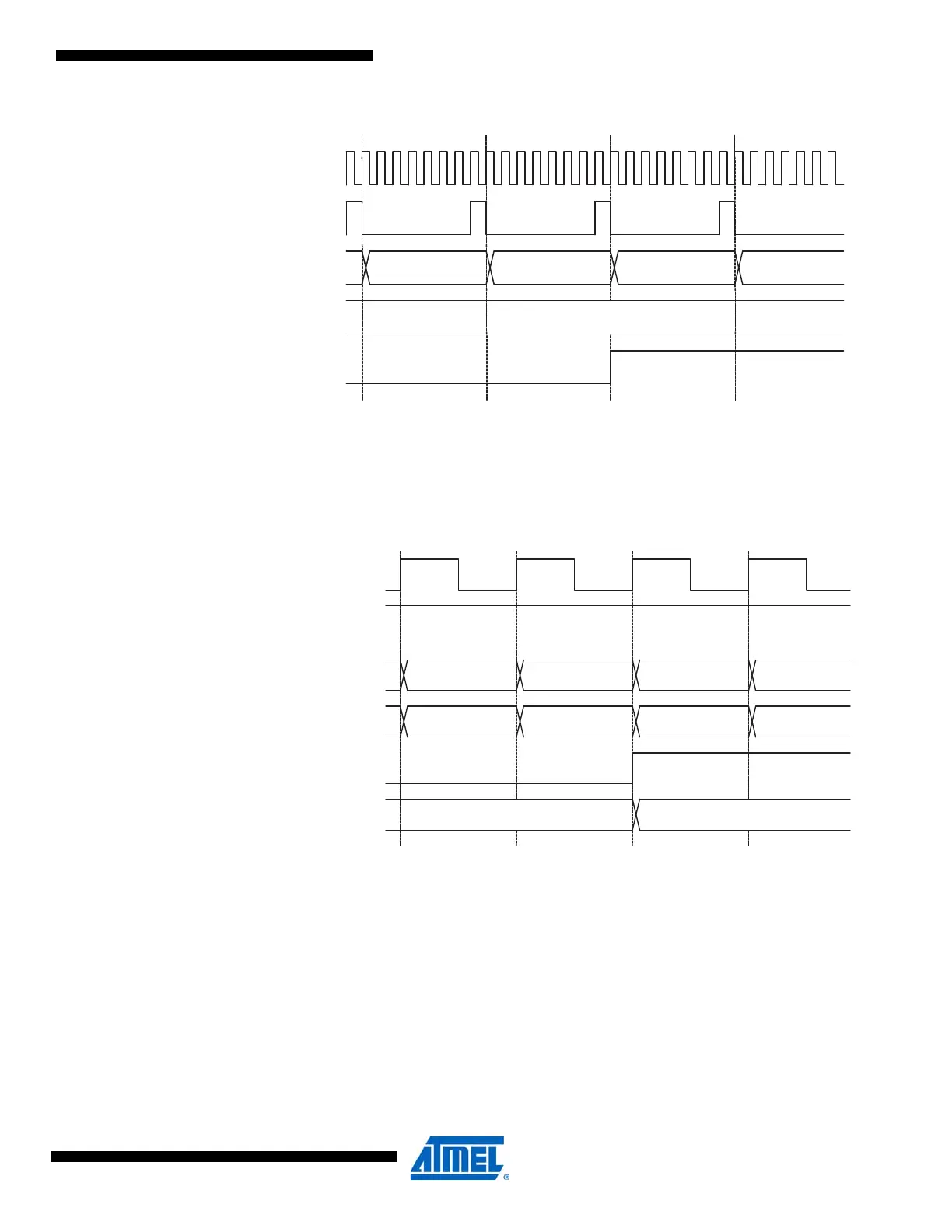
Figure 16-11. Timer/Counter Timing Diagram, Setting of OCF1x, with Prescaler (f
clk_I/O
/8)
Figure 16-12 shows the count sequence close to TOP in various modes. When using phase and
frequency correct PWM mode the OCR1x Register is updated at BOTTOM. The timing diagrams
will be the same, but TOP should be replaced by BOTTOM, TOP-1 by BOTTOM+1 and so on.
The same renaming applies for modes that set the TOV1 Flag at BOTTOM.
Figure 16-12. Timer/Counter Timing Diagram, no Prescaling
OCFnx
OCRnx
TCNTn
OCRnx Value
OCRnx - 1 OCRnx OCRnx + 1 OCRnx + 2
clk
I/O
clk
Tn
(clk
I/O
/8)
TOVn (FPWM)
and ICFn (if used
as TOP)
OCRnx
(Update at TOP)
TCNTn
(CTC and FPWM)
TCNTn
(PC and PFC PWM)
TOP - 1 TOP TOP - 1 TOP - 2
Old OCRnx Value
New OCRnx Value
TOP - 1 TOP BOTTOM BOTTOM + 1
clk
Tn
(clk
I/O
/1)
clk
I/O