314
8271D–AVR–05/11
ATmega48A/PA/88A/PA/168A/PA/328/P
not used, the used must wait at least t
WD_EEPROM
before issuing the next byte (See Table
28-18). In a chip erased device, no 0xFF in the data file(s) need to be programmed.
6. Any memory location can be verified by using the Read instruction which returns the con-
tent at the selected address at serial output MISO.
7. At the end of the programming session, RESET
can be set high to commence normal
operation.
8. Power-off sequence (if needed):
Set RESET
to “1”.
Tur n V
CC
power off.
28.8.3 Serial Programming Instruction set
Table 28-19 on page 314 and Figure 28-8 on page 316 describes the Instruction set.
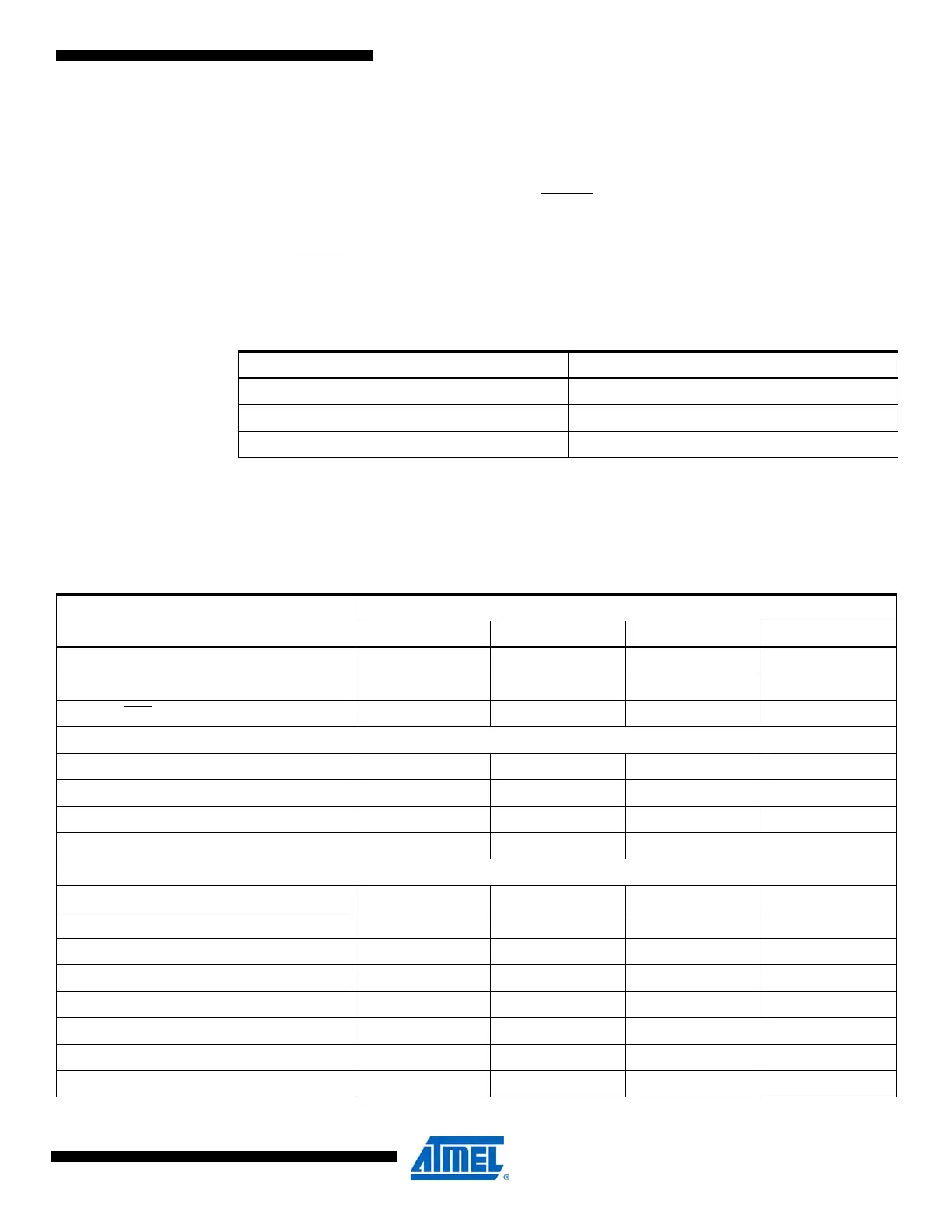
Table 28-18. Typical Wait Delay Before Writing the Next Flash or EEPROM Location
Symbol Minimum Wait Delay
t
WD_FLASH
4.5ms
t
WD_EEPROM
3.6ms
t
WD_ERASE
9.0ms
Table 28-19. Serial Programming Instruction Set (Hexadecimal values)
Instruction/Operation
Instruction Format
Byte 1 Byte 2 Byte 3 Byte4
Programming Enable $AC $53 $00 $00
Chip Erase (Program Memory/EEPROM) $AC $80 $00 $00
Poll RDY/BSY
$F0 $00 $00 data byte out
Load Instructions
Load Extended Address byte
(1)
$4D $00 Extended adr $00
Load Program Memory Page, High byte $48 $00 adr LSB high data byte in
Load Program Memory Page, Low byte $40 $00 adr LSB low data byte in
Load EEPROM Memory Page (page access) $C1 $00 0000 000aa data byte in
Read Instructions
Read Program Memory, High byte $28 adr MSB adr LSB high data byte out
Read Program Memory, Low byte $20 adr MSB adr LSB low data byte out
Read EEPROM Memory $A0 0000 00aa aaaa aaaa data byte out
Read Lock bits $58 $00 $00 data byte out
Read Signature Byte $30 $00 0000 000aa data byte out
Read Fuse bits $50 $00 $00 data byte out
Read Fuse High bits $58 $08 $00 data byte out
Read Extended Fuse Bits $50 $08 $00 data byte out