ATtiny10/11/12
71
Notes: 1. For compatibility with future devices, reserved bits should be written to zero if accessed. Reserved I/O memory addresses
should never be written.
2. Some of the status flags are cleared by writing a logical one to them. Note that the CBI and SBI instructions will operate on
all bits in the I/O register, writing a one back into any flag read as set, thus clearing the flag. The CBI and SBI instructions
work with registers $00 to $1F only.
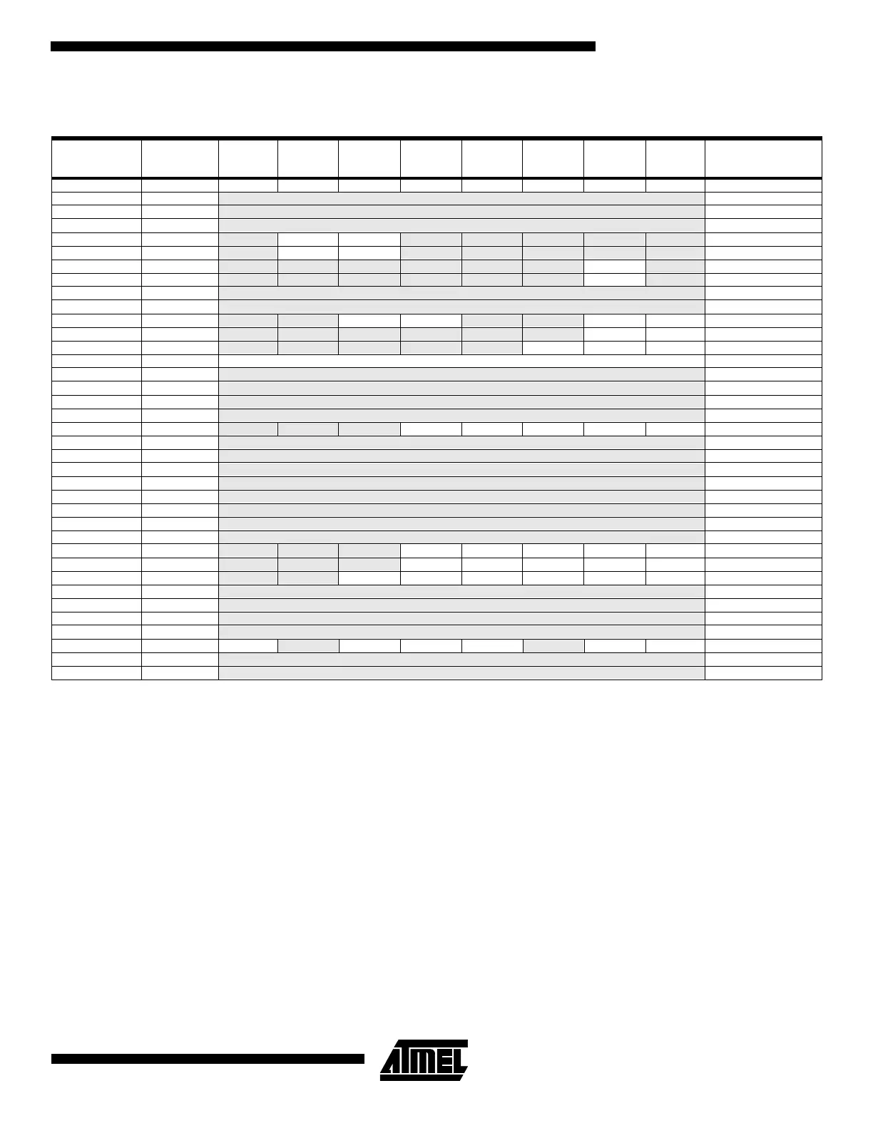
Register Summary ATtiny10/11
Address Name Bit 7 Bit 6 Bit 5 Bit 4 Bit 3 Bit 2 Bit 1 Bit 0 Page
$3F SREG I T H S V N Z C page 14
$3E Reserved
$3D Reserved
$3C Reserved
$3B GIMSK - INT0 PCIE - - - - - page 24
$3A GIFR
- INTF0 PCIF - - - - - page 25
$39 TIMSK
- - - - - - TOIE0 - page 25
$38 TIFR
- - - - - -TOV0- page 25
$37 Reserved
$36 Reserved
$35 MCUCR - -SESM- - ISC01 ISC00 page 26
$34 MCUSR
- - - - - - EXTRF PORF page 22
$33 TCCR0
- - - - - CS02 CS01 CS00 page 30
$32 TCNT0 Timer/Counter0 (8 Bit) page 31
$31 Reserved
$30 Reserved
... Reserved
$22 Reserved
$21 WDTCR - - - WDTOE WDE WDP2 WDP1 WDP0 page 31
$20 Reserved
$1F Reserved
$1E Reserved
$1D Reserved
$1C Reserved
$1B Reserved
$1A Reserved
$19 Reserved
$18 PORTB - - - PORTB4 PORTB3 PORTB2 PORTB1 PORTB0 page 37
$17 DDRB
- - - DDB4 DDB3 DDB2 DDB1 DDB0 page 37
$16 PINB
- - PINB5 PINB4 PINB3 PINB2 PINB1 PINB0 page 37
$15 Reserved
... Reserved
$0A Reserved
$09 Reserved
$08 ACSR ACD - ACO ACI ACIE - ACIS1 ACIS0 page 35
… Reserved
$00 Reserved
 Loading...


