ATtiny15L
10
I/O Memory
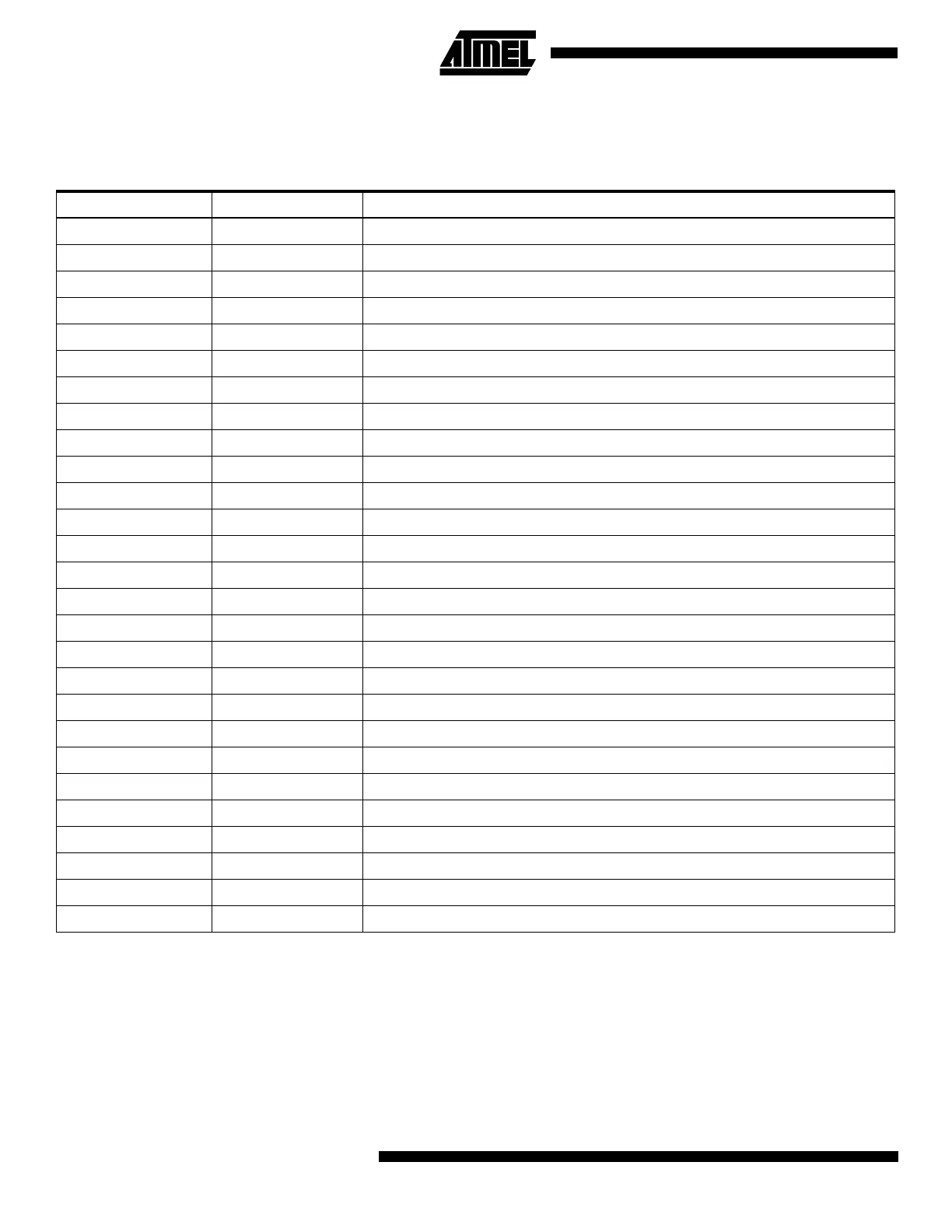
The I/O space definition of the ATtiny15L is shown in the following table:
Note: Reserved and unused locations are not shown in the table.
All ATtiny15L I/O and peripheral registers are placed in the I/O space. The I/O locations are accessed by the IN and OUT
instructions transferring data between the 32 general-purpose working registers and the I/O space. I/O registers within the
address range $00 - $1F are directly bit-accessible using the SBI and CBI instructions. In these registers, the value of sin-
gle bits can be checked by using the SBIS and SBIC instructions. Refer to the instruction set chapter for more details. For
compatibility with future devices, reserved bits should be written zero if accessed. Reserved I/O memory addresses should
never be written.
The I/O and peripheral control registers are explained in the following sections.
Table 2. ATtiny15L I/O Space
Address Hex Name Function
$3F SREG Status Register
$3B GIMSK General Interrupt Mask Register
$3A GIFR General Interrupt Flag Register
$39 TIMSK Timer/Counter Interrupt Mask Register
$38 TIFR Timer/Counter Interrupt Flag Register
$35 MCUCR MCU Control Register
$34 MCUSR MCU Status Register
$33 TCCR0 Timer/Counter0 Control Register
$32 TCNT0 Timer/Counter0 (8-bit)
$31 OSCCAL Oscillator Calibration Register
$30 TCCR1 Timer/Counter1 Control Register
$2F TCNT1 Timer/Counter1 (8-bit)
$2E OCR1A Timer/Counter1 Output Compare Register A
$2D OCR1B Timer/Counter1 Output Compare Register B
$2C SFIOR Special Function I/O Register
$21 WDTCR Watchdog Timer Control Register
$1E EEAR EEPROM Address Register
$1D EEDR EEPROM Data Register
$1C EECR EEPROM Control Register
$18 PORTB Data Register, Port B
$17 DDRB Data Direction Register, Port B
$16 PINB Input Pins, Port B
$08 ACSR Analog Comparator Control and Status Register
$07 ADMUX ADC Multiplexer Select Register
$06 ADCSR ADC Control and Status Register
$05 ADCH ADC Data Register High
$04 ADCL ADC Data Register Low