ATtiny15L
44
The ADC Data Register - ADCL and ADCH
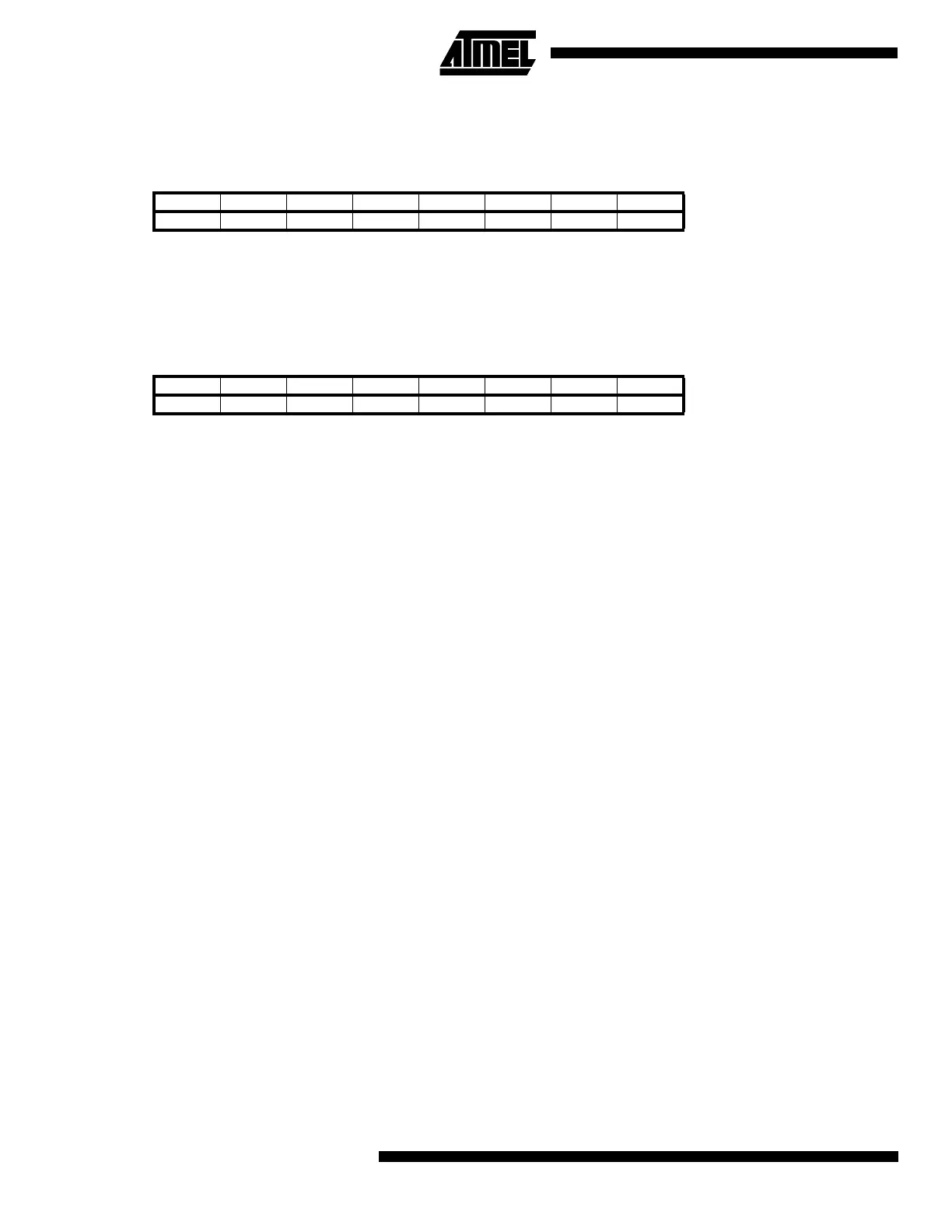
ADLAR = 0:
ADLAR = 1:
When an ADC conversion is complete, the result is found in these two registers. When ADCL is read, the ADC Data Regis-
ter is not updated until ADCH is read. If the result is left adjusted and no more than 8-bit precision is required, it is sufficient
to read ADCH. Otherwise, ADCL must be read first, then ADCH. The ADLAR bit in ADMUX affects the way the result is
read from the registers. If ADLAR is set, the result is left adjusted. If ADLAR is cleared (default), the result is right adjusted.
•
ADC9..0: ADC Conversion result
These bits represent the result from the conversion. For the differential channel, this is the value after gain adjustment, as
indicated in Table 19 on page 42. For single ended conversion, or if ADLAR or SIGN is zero, $000 represents ground, and
$3FF represents the selected reference voltage minus one LSB.
Scanning Multiple Channels
Since change of analog channel always is delayed until a conversion is finished, the Free Running mode can be used to
scan multiple channels without interrupting the converter. Typically, the ADC Conversion Complete interrupt will be used to
perform the channel shift. However, the user should take the following fact into consideration:
The interrupt triggers once the result is ready to be read. In Free Running mode, the next conversion will start immediately
when the interrupt triggers. If ADMUX is changed after the interrupt triggers, the next conversion has already started, and
the old setting is used.
ADC Noise Canceling Techniques
Digital circuitry inside and outside the ATtiny15L generates EMI which might affect the accuracy of analog measurements.
If conversion accuracy is critical, the noise level can be reduced by applying the following techniques:
1. The analog part of the ATtiny15L and all analog components in the application should have a separate analog
ground plane on the PCB. This ground plane is connected to the digital ground plane via a single point on the PCB.
2. Keep analog signal paths as short as possible. Make sure analog tracks run over the analog ground plane, and
keep them well away from high-speed switching digital tracks.
3. Use the ADC noise canceler function to reduce induced noise from the CPU.
4. If some Port B pins are used as digital outputs, it is essential that these do not switch while a conversion is in
progress.
Bit 151413121110 9 8
$05 - - - - - - ADC9 ADC8 ADCH
$04 ADC7 ADC6 ADC5 ADC4 ADC3 ADC2 ADC1 ADC0 ADCL
76543210
Read/Write RRRRRRRR
RRRRRRRR
Initial value 0 0 0 0 0 0 0 0
00000000
Bit 151413121110 9 8
$05 ADC9 ADC8 ADC7 ADC6 ADC5 ADC4 ADC3 ADC2 ADCH
$04 ADC1 ADC0 - - - - - - ADCL
76543210
Read/Write RRRRRRRR
RRRRRRRR
Initial value 0 0 0 0 0 0 0 0
00000000
 Loading...


