ATtiny15L
42
The ADC Multiplexer Selection Register – ADMUX
•
Bits 7..6 - REFS1..REFS0: Reference Selection Bits
These bits select the voltage reference for the ADC, as shown in Table 18. If these bits are changed during a conversion,
the change will not go in effect until this conversion is complete (ADIF in ADCSR is set). Whenever these bits are changed,
the next conversion will take 25 ADC clock cycles. If active channels are used, using AVCC or an external AREF higher
than (AVCC - 1V) is not recommended, as this will affect ADC accuracy. The internal voltage reference options may not be
used if an external reference voltage is being applied to the AREF pin.
•
Bit 5 - ADLAR: ADC Left Adjust Result
The ADLAR bit affects the presentation of the ADC conversion result in the ADC data register. If ADLAR is cleared, the
result is right adjusted. If ADLAR is set, the result is left adjusted. Changing the ADLAR bit will affect the ADC data register
immediately, regardless of any ongoing conversions. For a complete description of this bit, see “The ADC Data Register -
ADCL and ADCH” on page 44.
•
Bits 4..3 - Res: Reserved Bits
These bits are reserved bits in the ATtiny15L and always read as zero.
•
Bits 2..0 - MUX2..MUX0: Analog Channel and Gain Selection Bits 2..0
The value of these bits selects which analog input is connected to the ADC. In case of differential input (PB3 - PB4), gain
selection is also made with these bits. Selecting PB3 as both inputs to the differential gain stage enables offset measure-
ments. Refer to Table 19 for details. If these bits are changed during a conversion, the change will not go into effect until
this conversion is complete (ADIF in ADCSR is set).
Note: 1. For offset calibration only. See “Operation” on page 38.
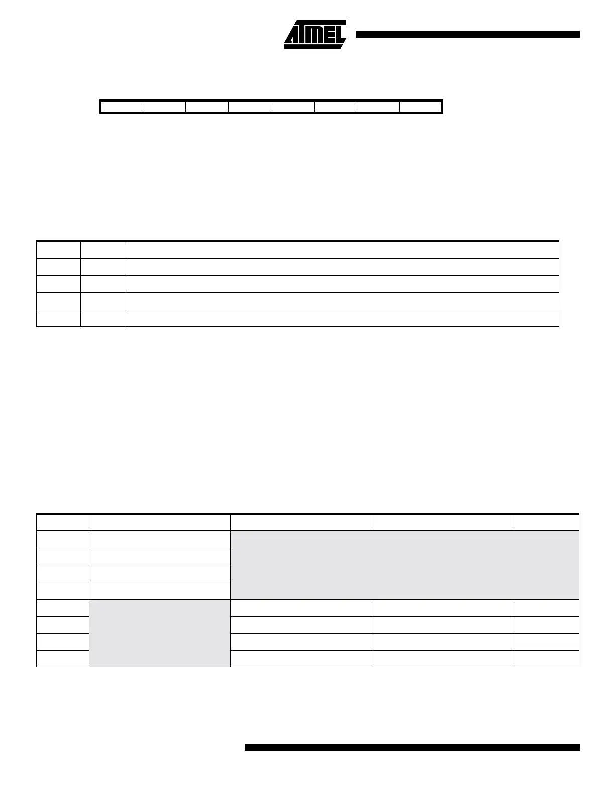
Bit 76543210
$07 REFS1 REFS0 ADLAR - - MUX2 MUX1 MUX0 ADMUX
Read/Write R/W R/W R/W R R R/W R/W R/W
Initial value 0 0 0 0 0 0 0 0
Table 18. Voltage Reference Selections for ADC
REFS1 REFS0 Voltage Reference Selection
0 0 VCC used as analog reference, disconnected from PB0 (AREF)
0 1 External Voltage Reference at PB0 (AREF) pin, Internal Voltage Reference turned off
1 0 Internal Voltage Reference without external bypass capacitor, disconnected from PB0 (AREF)
1 1 Internal Voltage Reference with external bypass capacitor at PB0 (AREF) pin
Table 19. Input Channel and Gain Selections
MUX2..0 Single Ended Input Positive Differential Input Negative Differential Input Gain
000 ADC0 (PB5)
N/A
001 ADC1 (PB2)
010 ADC2 (PB3)
011 ADC3 (PB4)
100
(1)
N/A
ADC2 (PB3) ADC2 (PB3) 1x
101
(1)
ADC2 (PB3) ADC2 (PB3) 20x
110 ADC2 (PB3) ADC3 (PB4) 1x
111 ADC2 (PB3) ADC3 (PB4) 20x
 Loading...


