ATtiny15L
39
The ADC is enabled by setting the ADC Enable bit, ADEN in ADCSR. Voltage reference and input channel selections will
not go into effect until ADEN is set. The ADC does not consume power when ADEN is cleared, so it is recommended to
switch off the ADC before entering power-saving sleep modes.
A conversion is started by writing a logical one to the ADC Start Conversion bit, ADSC. This bit stays high as long as the
conversion is in progress and will be set to zero by hardware when the conversion is completed. If a different data channel
is selected while a conversion is in progress, the ADC will finish the current conversion before performing the channel
change.
The ADC generates a 10-bit result, which is presented in the ADC data registers, ADCH and ADCL. By default, the result is
presented right adjusted, but can optionally be presented left adjusted by setting the ADLAR bit in ADMUX.
If the result is left adjusted and no more than 8-bit precision is required, it is sufficient to read ADCH. Otherwise, ADCL
must be read first, then ADCH, to ensure that the content of the data registers belongs to the same conversion. Once
ADCL is read, ADC access to data registers is blocked. This means that if ADCL has been read, and a conversion com-
pletes before ADCH is read, neither register is updated and the result from the conversion is lost. When ADCH is read,
ADC access to the ADCH and ADCL registers is re-enabled.
The ADC has its own interrupt which can be triggered when a conversion completes. When ADC access to the data regis-
ters is prohibited between reading of ADCH and ADCL, the interrupt will trigger even if the result is lost.
Prescaling and Conversion Timing
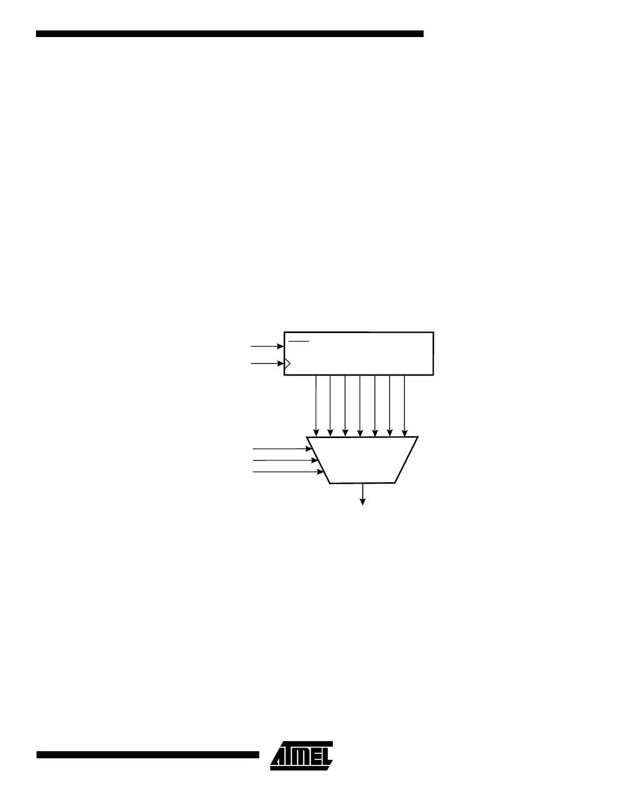
Figure 26. ADC Prescaler
The successive approximation circuitry requires an input clock frequency between 50 kHz and 200 kHz. Using a higher
input frequency will affect the conversion accuracy, see “ADC Characteristics” on page 45. The ADC module contains a
prescaler, which divides the system clock to an acceptable ADC clock frequency.
The ADPSn bits in ADCSR are used to generate a proper ADC clock input frequency from any CK frequency above 100
kHz. The prescaler starts counting from the moment the ADC is switched on by setting the ADEN bit in ADCSR. The pres-
caler keeps running for as long as the ADEN bit is set, and is continuously reset when ADEN is low.
When initiating a conversion by setting the ADSC bit in ADCSR, the conversion starts at the following rising edge of the
ADC clock cycle. If differential channels are selected, the conversion will only start at every other rising edge of the ADC
clock cycle after ADEN was set.
A normal conversion takes 13 ADC clock cycles. In certain situations, the ADC needs more clock cycles to perform initial-
ization and minimize offset errors. These extended conversions take 25 ADC clock cycles and occur as the first conversion
after one of the following events:
• the ADC is switched on (ADEN in ADCSR is set)
• the voltage reference source is changed (the REFS1..0 bits in ADMUX change value)
• a differential channel is selected (MUX2 in ADMUX is “1”). Note that subsequent conversions on the same channel are
not extended conversions.
7-BIT ADC PRESCALER
CK
ADPS0
ADPS1
ADPS2
CK/128
CK/2
CK/4
CK/8
CK/16
CK/32
CK/64
Reset
ADEN
 Loading...


