ATtiny15L
9
Subroutine and Interrupt Hardware Stack
The ATtiny15L uses a 3-level deep hardware stack for subroutines and interrupts. The hardware stack is 9-bit wide and
stores the Program Counter (PC) return address while subroutines and interrupts are executed.
RCALL instructions and interrupts push the PC return address onto stack level 0, and the data in the other stack levels 1-2
are pushed one level deeper in the stack. When a RET or RETI instruction is executed the returning PC is fetched from
stack level 0, and the data in the other stack levels 1-2 are popped one level in the stack.
If more than 3 subsequent subroutine calls or interrupts are executed, the first values written to the stack are overwritten.
Pushing four return addresses A1, A2, A3, and A4 followed by four subroutine or interrupt returns, will pop A4, A3, A2, and
once more A2 from the hardware stack.
The EEPROM Data Memory
The ATtiny15L contains 64 bytes of data EEPROM memory. It is organized as a separate data space, in which single bytes
can be read and written. The EEPROM has an endurance of at least 100,000 write/erase cycles. The access between the
EEPROM and the CPU is described on page 25, specifying the EEPROM Address Register, the EEPROM Data Register,
and the EEPROM Control Register.
Memory Access and Instruction Execution Timing
This section describes the general access timing concepts for instruction execution and internal memory access.
The AVR CPU is driven by the System Clock Ø, directly generated from the external clock crystal for the chip. No internal
clock division is used.
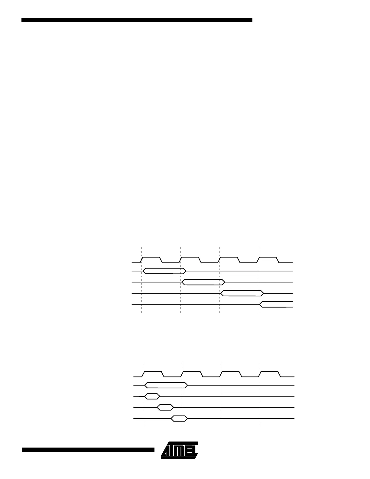
Figure 10 shows the parallel instruction fetches and instruction executions enabled by the Harvard architecture and the
fast-access register file concept. This is the basic pipelining concept to obtain up to 1 MIPS per MHz with the corresponding
unique results for functions per cost, functions per clocks, and functions per power-unit.
Figure 10. The Parallel Instruction Fetches and Instruction Executions
Figure 11 shows the internal timing concept for the register file. In a single-clock cycle an ALU operation using two register
operands is executed, and the result is stored back to the destination register.
Figure 11. Single Cycle ALU Operation
System Clock Ø
1st Instruction Fetch
1st Instruction Execute
2nd Instruction Fetch
2nd Instruction Execute
3rd Instruction Fetch
3rd Instruction Execute
4th Instruction Fetch
T1 T2 T3 T4
System Clock Ø
Total Execution Time
Register Operands Fetch
ALU Operation Execute
Result Write Back
T1 T2 T3 T4

 Loading...


