ATtiny15L
29
•
Bits 3,2,1,0 - CS13, CS12, CS11, CS10: Clock Select bits 3, 2, 1, and 0
The Clock Select bits 3, 2, 1, and 0 define the prescaling source of Timer/Counter1.
The Stop condition provides a Timer Enable/Disable function. The prescaled CK modes are scaled directly from the CK
oscillator clock.
The Timer/Counter1 – TCNT1
This 8-bit register contains the value of Timer/Counter1.
Timer/Counter1 is implemented as an up-counter with read and write access. Due to synchronization of the CPU and
Timer/Counter1, data written into Timer/Counter1 is delayed by one CPU clock cycle.
Timer/Counter1 Output Compare RegisterA – OCR1A
The Output Compare Register 1A is an 8-bit read/write register.
The Timer/Counter Output Compare Register 1A contains the data to be continuously compared with Timer/Counter1.
Actions on compare matches are specified in TCCR1. A compare match does only occur if Timer/Counter1 counts to the
OCR1A value. A software write that sets TCNT1 and OCR1A to the same value does not generate a compare match.
A compare match will set (one) the compare interrupt flag in the CPU clock cycle following the compare event.
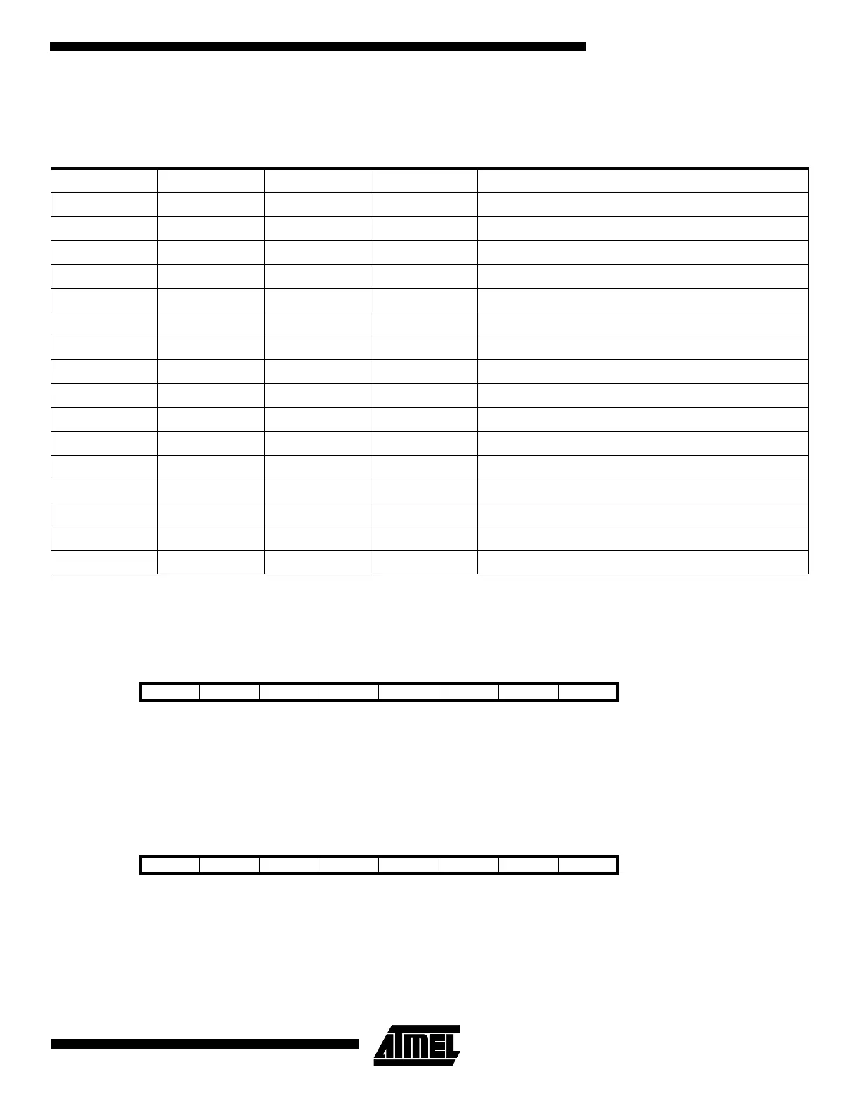
Table 11. Timer/Counter1 Prescale Select
CS13 CS12 CS11 CS10 Description
0 0 0 0 Timer/Counter1 is stopped.
0 0 0 1 CK*16 (=PCK)
0 0 1 0 CK*8 (=PCK/2)
0 0 1 1 CK*4 (=PCK/4)
0 1 0 0 CK*2 (=PCK/8)
0101CK
0110CK/2
0111CK/4
1000CK/8
1001CK/16
1010CK/32
1011CK/64
1100CK/128
1101CK/256
1110CK/512
1 1 1 1 CK/1024
Bit 76543210
$2F MSB LSB TCNT1
Read/Write R/W R/W R/W R/W R/W R/W R/W R/W
Initial value 0 0 0 0 0 0 0 0
Bit 76543210
$2E MSB LSB OCR1A
Read/Write R/W R/W R/W R/W R/W R/W R/W R/W
Initial value 0 0 0 0 0 0 0 0
 Loading...


