61
SAMA5D3x-EK User Guide [USER GUIDE]
11180B–ATARM–29-Oct-13
5.2.3.1 Disabling J-Link-OB-ATSAM3U4C
Jumper JP15 disables the J-Link-OB-ATSAM3U4C JTAG functionality. When the jumper is installed, it grounds Pin 25 of
the ATSAM3U4C that is normally pulled high. This signals to the microcontroller it must not provide JTAG support.
Jumper JP15 not installed: J-Link-OB-ATSAM3U4C is enabled and fully functional
Jumper JP15 installed: JTAG functionality is disabled
Jumper J15 disables only J-Link functionality. The debug serial port (DBGU) that is emulated through a communication
device class (CDC) of the same USB connector remains operational.
The built-in JTAG controller does not have to be explicitly disabled to use an external JTAG controller through the 20-pin
JTAG port. The internal J-Link-OB connects to a target only after it receives a first command; otherwise, it remains
disabled.
5.2.3.2 Hardware UART via CDC
In addition to J-Link-OB functionality, the ATSAM3U4C microcontroller LAO provides a bridge to a debug serial port
(DBGU) of the processor on a CM board. The port is made accessible over the same USB connection used by JTAG by
implementing communication device class (CDC), which allows terminal communication with the target device.
This feature is enabled only if the microcontroller Pin 24 is not grounded. The pin is normally pulled high and controlled
by jumper JP16.
Jumper JP16 not installed: the device is enabled
Jumper JP16 installed: the CDC device is disabled
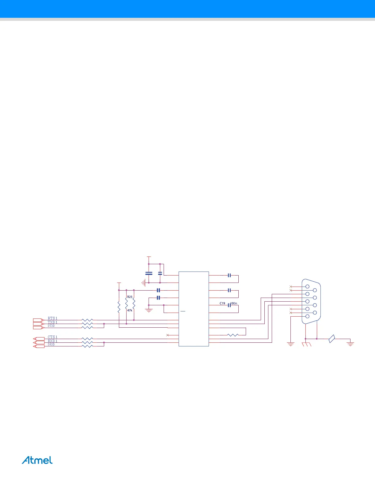
5.2.4 USART
The USART1 is used as a user serial communication port. This USART provides an RS-232 interface with transceiver
TXD, RXD lines and hardware flow control CTS/RTS lines. The device uses a DB-9 male connector. The software must
drive the appropriate PIO pins to enable the USART function.
Figure 5-7. USART1 Com Port
RTSC1
TXDC1
CTSC1
RXDC1
EARTH_RS232
VDDIOP1
VDDIOP1
PB27
PB29
PB28
PB26
PB31
PB30
USART1
RTS1
TXD1
CTS1
RXD1
DRXD
DTXD
R23
47k
R23
47k
C19 100nC19 100n
J8J8
5
4
3
2
1
9
8
7
6
10
11
R132 0R
DNP
R132 0R
DNP
C15 100nC15 100n
C17 100nC17 100n
R28 0RR28 0R
C14
100n
C14
100n
C13
4.7u
C13
4.7u
C18 100nC18 100n
R31 0RR31 0R
R133 0R
DNP
R133 0R
DNP
R30 0RR30 0R
L5
220ohm at 100MHz
L5
220ohm at 100MHz
1 2
MN4
ADM3312EARU
MN4
ADM3312EARU
V+
1
C2+
2
VCC
3
C2-
4
EN
5
C1+
6
T1IN
7
T2IN
8
T3IN
9
R1OUT
10
R2OUT
11
R3OUT
12
R3IN
13
R2IN
14
R1IN
15
T3OUT
16
T2OUT
17
T1OUT
18
SD
19
C1-
20
V-
21
C3-
22
GND
23
C3+
24
R27 0RR27 0R
R22
47k
R22
47k
C16 100nC16 100n
R29 0RR29 0R
R24
47k
R24
47k
 Loading...