Section 4 Theory of Operation
4-6
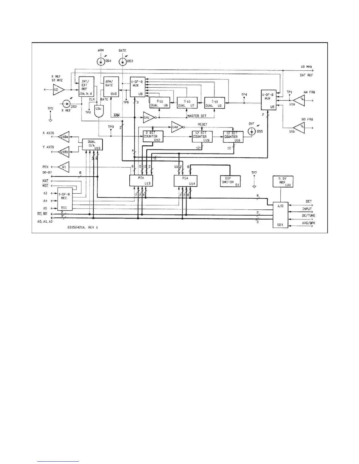
Figure 4-4. Frequency Counter Circuits Block Diagram
4-25. The RAM is powered from a non-volatile power
supply consisting of Q1, CR1 and BT1 (TP9). If a power
fault occurs, circuits in the power supply activate the
SNMI line which in turn activates the NMI processor in-
terrupt line (TP7). This causes the processor to stop the
control program and execute a HALT instruction which
sets the HALT pin low. This inhibits further write cycles to
the RAM by setting a latch formed by U6c and d which
disconnects the chip select (CS) line to the RAM using
analog switch U5. Signal PRST is also set low shortly
after SNMI is activated, causing the CPU to be reset to
the program start. When proper operating voltage is
restored, the SNMI line returns high releasing NMI and
restoring the RAM CS connection. During the power
down interval the RAM is powered by BT1 (TP9).
4-26. Microprocessor timing is controlled by a 5 MHz
clock (TP1) which is derived from a 10 MHz TCXO, Y1,
and flip-flop divider U13a. The 5 MHz clock signal is also
used by the IEEE-488 microcontroller, U16. The 10 MHz
TCXO output is also buffered through U2a and is used for
the internal timebase reference for the frequency counter
circuits.
4-27. All IEEE-488 interface operations are conducted by
U16 in conjunction with the microprocessor interrupt
routines. These routines move data into and out of mem
ory buffers as required in response to bus commands.
U17 and U18 are buffer circuits which connect U16 to the
IEEE-488 bus via J20. These buffers meet the electrical
requirements of the IEEE-488.
4-28. Interrupt oriented control enables the CPU and
control program to respond quickly to peripheral activity.
When bus activity occurs, U16 sets the INT line (TP8) via
U1e, U2b and U1c. When a display/keyboard interrupt
occurs the KEY INT line sets the microprocessor interrupt
line through U2b and U1c. The microprocessor
determines the source of the interrupt by reading the
interrupt status buffer, U8, and services the requesting
peripheral device.
4-29. The instrument bus interface adapter consists of
U3, U9, R8, and R9. These tri-state buffers are normally
in the high-impedance mode during all memory transfers
and I/O data transfers occurring between the CPU and
the display/keyboard circuits or the IEEE-488 interface.
4-30. The display/keyboard bus interface adapter con-
sists of U4 and U10. These tri-state buffers are only active
during display/keyboard circuit transactions.


 To Next Page