Section 4 Theory of Operation
4-12
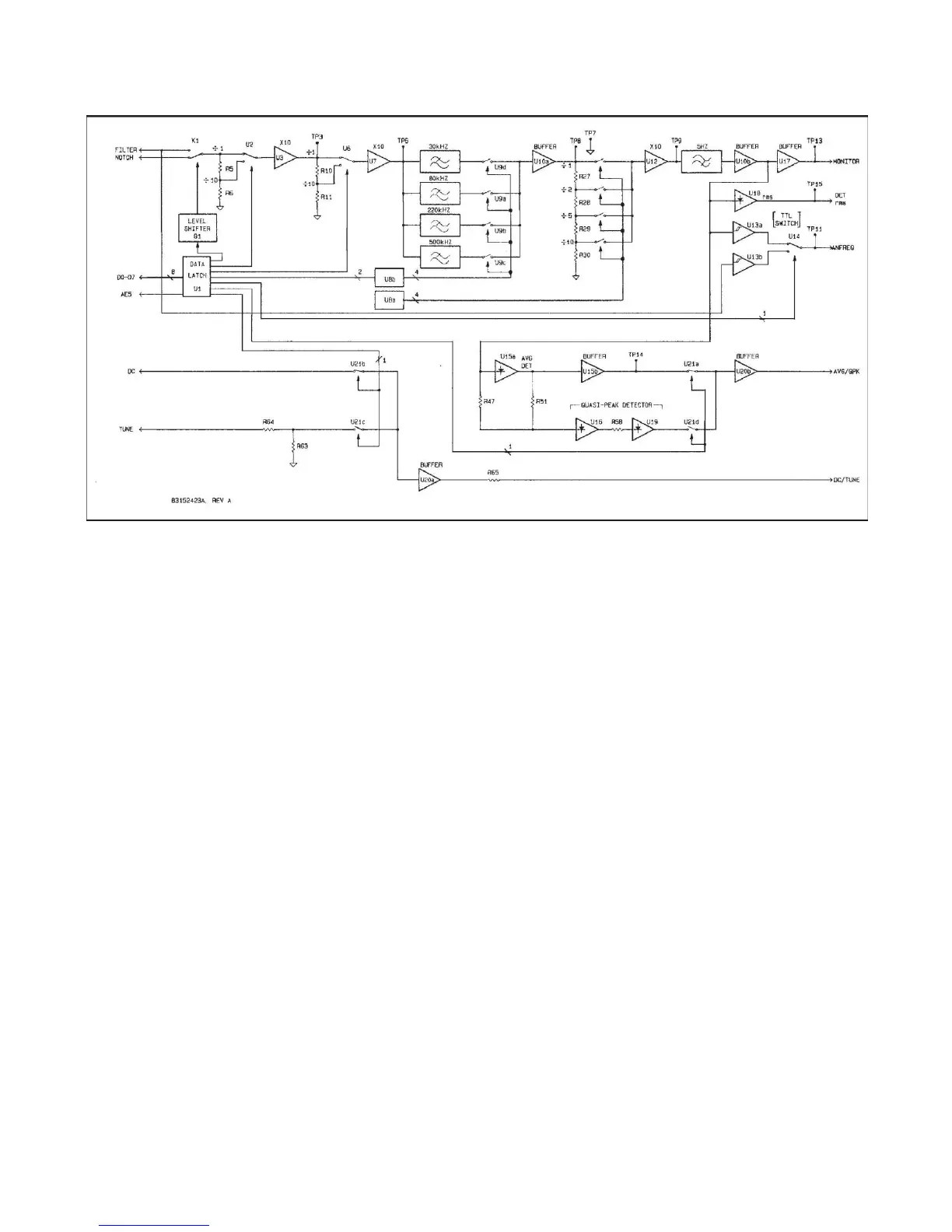
Figure 4-8. Detector Circuits Block Diagram.
4-63. Following U7 (TP6) are the low-pass filter selec-
tions. Analog switches U9a through d select the various
filter values for the 30 kHz, 80 kHz, 220 kHz or 500 kHz
low-pass filters. Unity gain buffer U10a completes the
selected filter (TP8). The output of U10a (TP8) is AC
coupled to a final programmable attenuator consisting of
analog switch U11a through d and R27 thorugh R33.
Amplifier U12 is an identical clamped gain stage as U3
and U7 with a gain of 20 dB. The combination of the at-
tenuator and amplifier form a programmable gain stage
with gain selections of X1, X2, X5, and X10.
4-64. Amplifier U10b and associated components form a
5 Hz high-pass filter which determines the low frequency
bandwidth of the Model 1121A. Buffer amplifier U17 and
CR14, CR15 and R55 present the detector output signal
to the rear panel MONITOR output connector for external
analysis (TP13).
4-65. The complete detector amplifier and attenuator
chain is programmable for a gain change of 0 to 60 dB in
1X, 2X, or 5X increments. In the distortion and SINAD
modes the 20 dB amplifier on the notch filter plug-in board
increases the chain to a total combined gain of 80 dB. The
programmable gain is required to maintain a constant
level of between 1.2 and 3 volts at the rms, average and
quasi-peak detectors to preserve the resolution and
accuracy of the analyzer over a wide dynamic range. The
rms detector consists of U18 and associated
components. The output of the rms detector (TP15) is a
DC level equal in amplitude to the rms value of the input
signal.
4-66. The quasi-peak detector consists of U16 and U19
and associated components. U16 forms an integrator with
an attack time of less than 2 ms and decay time of 400
ms. U19 forms an integrator with an attack time of 200 ms
and decay time of 600 ms. The average detector consists
of U15a and b and associated components. U15a forms a
full wave rectifier circuit and C56 filters the output to a DC
level representing the average value of the input signal
(TP14). Analog switch U21 selects either the average or
quasi-peak detector for measurement by one channel of
the A/D converter on the counter plug-in board. Resistors
R37 and R37 balance the gain of the average and rms
detectors to be equal for a sine-wave input waveform.
Inverting amplifier U13b presents a positive 0 to 3 volt
level to the A/D converter (TP7).


 To Next Page