EasyManua.ls Logo

CHINT NVF2G Series - Page 21

CHINT NVF2G Series
116 pages
Print Icon
To Next Page IconTo Next Page
To Previous Page IconTo Previous Page
Loading...
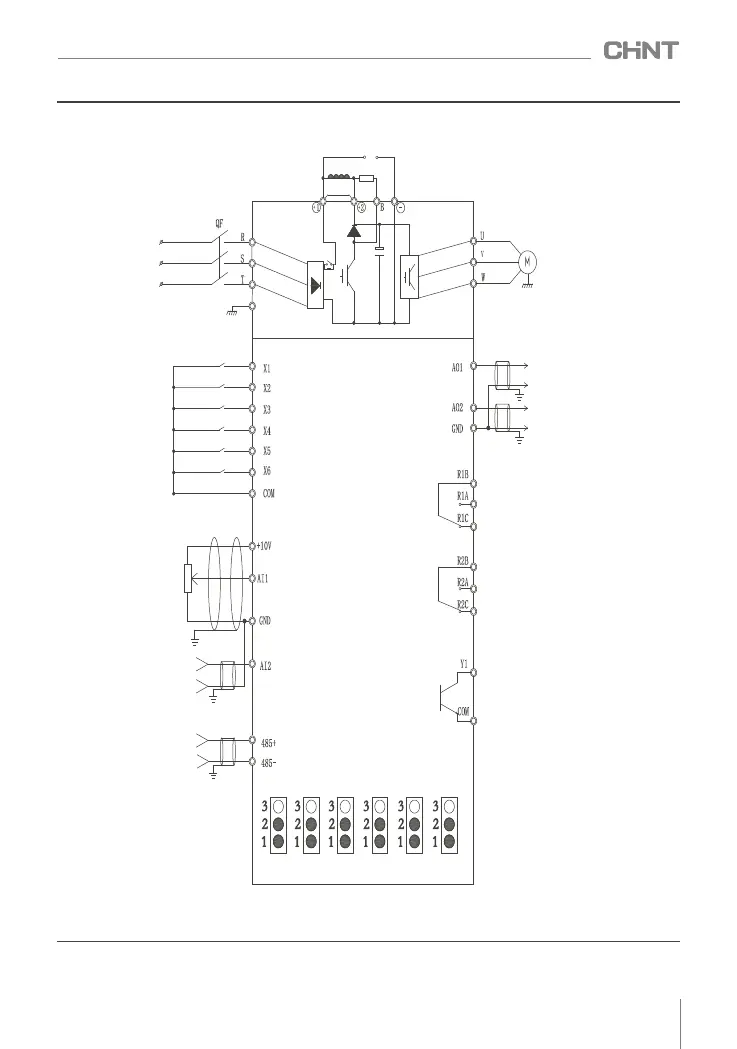
Figure 4.12 NVF2G-1.5/PS4~NVF2G-400/TS4 Wiring Diagram
4.3.2 Control terminal description
   ( 1) Jumper selection
013
NVF2G Series Inverter User's Guide
3
2
1
3
2
1
3
2
1
3
2
1
J601 J602 J603 J604
3
2
1
J605
3
2
1
J606
Braking Unit
External braking Resistor
DC Reactor
A Short Jumper
AC
Input
Inverter Earth
Motor Earth
Multi-functional 1
Multi-functional 2
Multi-functional 3
Multi-functional 4
Multi-functional 5
Multi-functional 6
Multi-functional
Analog 0utput 1
(0-10) V or (0/4-20) mA
Multi-functional
Analog 0utput 2
(0-10) V or (0/4-20) mA
Multi-functional
Relay 0utput 1
Contact Capacity:
AC 250V 3A
Resister for
Frequency
(0-10) V or
(0/4-20)mA
Multi-functional
Relay Output 2
Contact Capacity:
AC 250V 3A
Analog Input
(0-10) V or
(0/4-20)mA
Open Collector Output
(DC 24V)
RS485 Communication
Modbus Communication

Table of Contents