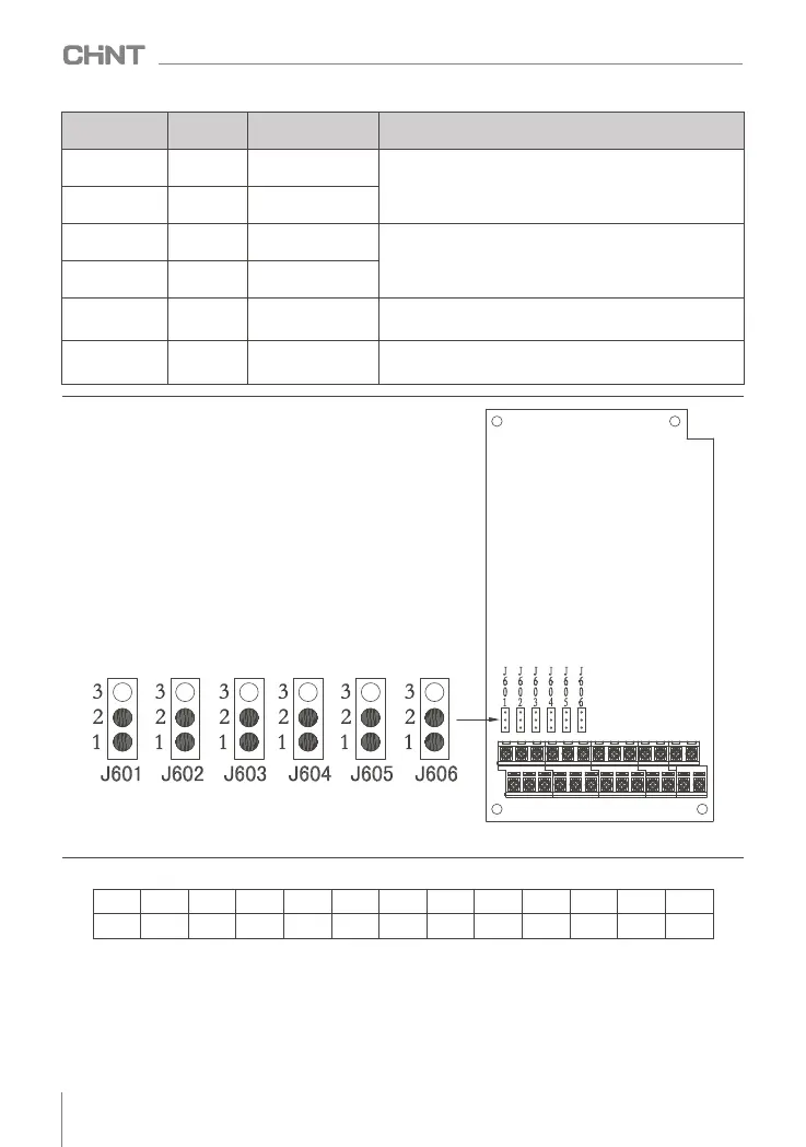
Function
Jumper
terminal
Shorting location
and definition
Illustrate
AI1
J601
1-2 : V
2-3 : I
V voltage type analog input range : ( -10~ + 10 ) V;
I Current analog input range : ( 0~20) mA or (4~20) mA
Default to V voltage type
AI2
J602
1-2:V
2-3 : I
AO1
J603
1-2 : V
2-3 : I
V voltage type analog output range : (-10~ + 10)V;
I Current analog output range : (0~20) mA or (4~20) mA
Default to V voltage type
AO2 J604
1-2 : V
2-3 : I
485 terminal
matching
resistance
J605
1-2 : no access
2-3 : access
Matching resistor 4.7kΩ Default not connected
X1-X6
interface mode
J606
1-2: PNP
2-3: NPN
Default is PNP type
Figure 4.13 Jumper position
(2) The terminal arrangement of the control circuit is shown in Figure 4.14 below :
Figure 4.14 Arrangement of inverter control circuit terminals
4.3.3 Control terminal function description
485+ 485-
X1
X2
X3 X4
X5
X6
Y1
COM
R2A R2B
R2C
+10V
AI2
AI1
GND
AO1
AO2 GND COM
+24V
R1A
R1B
R1C
014
NVF2G Series Inverter User's Guide