150
130
110
90
70
50
30
10
2
4
6
8
RESISTANCE (OHMS)
RESISTANCE BARS
Figure 6.4 Resistance vs. Bargraph
6-19
a drive time that occurs on the diode of U6. A
logic device on the Display Assembly drives this
diode with a square wave, and when this diode is
conducting current, and if ABC™ is requested ,
then both U8 and U9 will be switched on and the
collectors of both will go low.
mizing the RF voltage appearing across T4 wind
-
ings. T4 also acts to step-up the return imped
-
ance by about 10:1.
The A.R.M. oscillator generates a low power sin
-
ewave voltage of about 36 KHz. This frequency
is determined by the inductance of T2 in paral
-
lel with C25, and that of C27 and C30 reflected
through T4. Transistors Q2 and Q3 are cross
coupled via R28 and R32, so that when one tran
-
sistor is conducting, the other is off due to lack of
base drive. The conducting transistor turns off at
the next zero crossing of the sinusoidal voltage on
the primary of T2. This allows its collector volt
-
age to rise and thus provide base current to the
other transistor to switch on. The collector volt
-
ages appear like half-wave rectified AC, with each
collector 180 degrees out of phase.
The A.R.M. oscillator is powered by a constant
0.5mA DC current driven from the V
ARM signal
line. This current feeds into the center tap of T2
primary. The voltage on the center tap is the aver
-
age of the two collector voltages, so it appears
as a full-wave rectified sinewave. Inductor L1
holds the current supplied to T2 constant regard
-
less of these voltage variations, while C18 serves
as a bypass to limit the noise conducted from the
VARM line to the amplifier, U1D.
Diode VR2 is a +1.235V regulator whose output
voltage appears across the 2.49K ohm resistor
R20, thus driving a constant current of 0.5mA in
the V
ARM line. The voltage at TP3 is a 2X VARM
as U1D is a 2X amplifier.
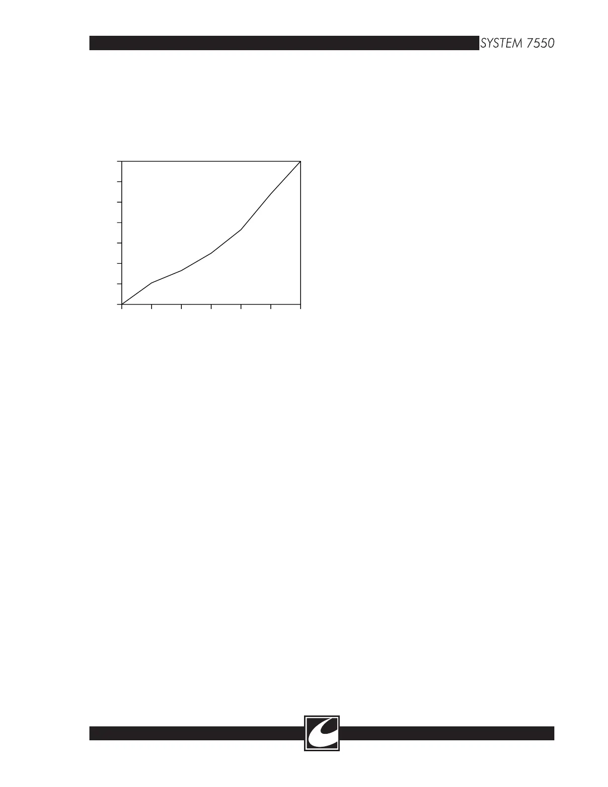
The ASSIST resistance indicator (bargraph) will
be illuminated when the pad resistance is 10 to
150 ohms. At just over 10 ohms, the two left
segments are illuminated. As V
ARM increases,
additional segments illuminate in proportion to
VARM, progressing to the right until the resistance
approaches 150 ohms, where eight bars are illumi
-
nated. When the resistance exceeds 150 ohms, all
ten segments are illuminated.
In Dual Foil Mode, the microprocessor declares a
Return Fault if the resistance is less than 10 ohms
or greater than 150 ohms. If V
ARM is within
acceptable limits (10 - 150 ohms), the Return
Fault Indicator will turn off when the Monitor
Set switch is pressed. A Return Fault is declared
when the resistance increases about 20% above
the stored value or goes out of range. When a
Return Fault condition occurs, and if the resis
-
tance is within acceptable 2V
ARM limits, the new
6.11.2 Aspen Return Monitor (A.R.M.)
The A.R.M. circuit converts the electrical resis
-
tance appearing in the return electrode circuit
into a digital value which can be processed by the
microprocessor. Software processes use this value
in conjunction with the SINGLE PAD/DUAL
PAD and MONITOR SET/ buttons to determine
when a RETURN FAULT condition exists. The
ASSIST resistance indicator is also driven by soft
-
ware to indicate the value of the measured DUAL
FOIL resistance in the 10 to 150 ohm range.
Figure 6.4 shows the approximate resistance vs.
number of illuminated bars in the resistance indi
-
cator. If no bars are lit, then the resistance is less
than approximately 10 ohms, and if 10 bars are
lit, the resistance is greater than approximately
150 ohms. It is not possible for just 1 or 9 bars
to be lit, unless a segment has failed.
The Handsense/A.R.M. schematic (Figure C-20)
contains the A.R.M. circuitry. It is comprised of
an oscillator section and an isolation section. The
isolation section employs a toroidal transformer,
T4, to couple the return electrode impedance to
the A.R.M. oscillator while isolating that circuit
from the effects of applied RF electrosurgical cur
-
rent and voltage. C27 and C30 split the return
current evenly between the two legs, thus mini
-