MB95710M Series
MB95770M Series
Document Number: 002-09307 Rev. *D Page 107 of 172
19.5.3 Port 9 registers
• Port 9 register functions
• Correspondence between registers and pins for port 9
19.5.4 Port 9 operations
• Operation as an output port
• A pin becomes an output port if the bit in the DDR9 register corresponding to that pin is set to “1”.
• When a pin is used as an output port, it outputs the value of the PDR9 register to external pins.
• If data is written to the PDR9 register, the value is stored in the output latch and is output to the pin set as an output
port as it is.
• Reading the PDR9 register returns the PDR9 register value.
• To use a pin shared with the LCDC as an output port, set the bit corresponding to that pin in the VE[4:1] bits in the
LCDC enable register 1 (LCDCE1) to “0” to select the general-purpose I/O port function.
• Operation as an input port
• A pin becomes an input port if the bit in the DDR9 register corresponding to that pin is set to “0”.
• If data is written to the PDR9 register, the value is stored in the output latch but is not output to the pin set as an
input port.
• Reading the PDR9 register returns the pin value. However, if the read-modify-write (RMW) type of instruction is
used to read the PDR9 register, the PDR9 register value is returned.
• To use a pin shared with the LCDC as an input port, set the bit corresponding to that pin in the VE[4:1] bits in the
LCDCE1 register to “0” to select the general-purpose I/O port function.
• Operation at reset
If the CPU is reset, all bits in the DDR9 register are initialized to “0” and port input is enabled.
• Operation in stop mode and watch mode
• If the pin state setting bit in the standby control register (STBC:SPL) is set to “1” and the device transits to stop
mode or watch mode, the pin is compulsorily made to enter the high impedance state regardless of the DDR9 reg-
ister value. The input of that pin is locked to “L” level and blocked in order to prevent leaks due to input open.
• If the pin state setting bit is “0”, the state of the port I/O or that of the peripheral function I/O remains unchanged
and the output level is maintained.
• Operation as an LCD drive power supply pin
• Set the bit in the DDR9 register corresponding to an LCD drive power supply pin to “0”.
• To use a pin shared with a general-purpose I/O port as an LCD drive power supply pin, set the bit corresponding
to that pin in the VE[4:1] bits in the LCDCE1 register to “1” to select the LCD drive power supply function.
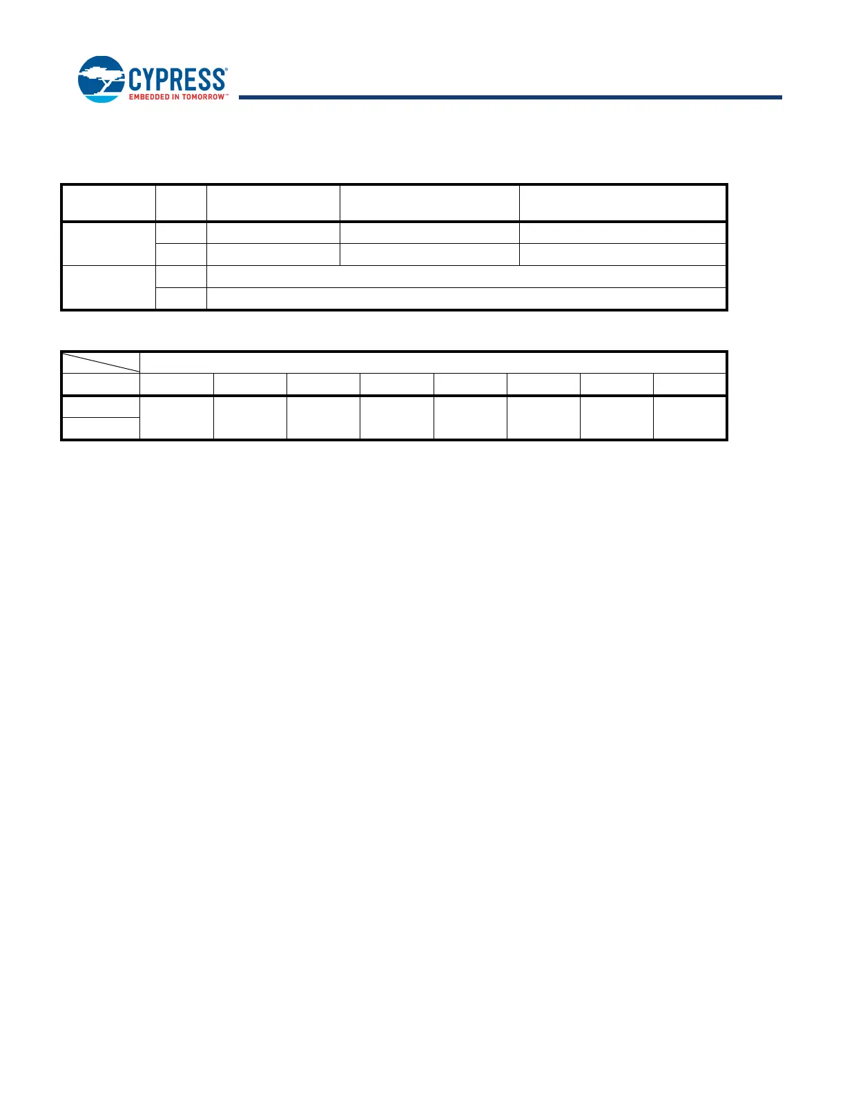
Register
abbreviation
Data Read
Read by read-modify-write
(RMW) instruction
Write
PDR9
0 Pin state is “L” level. PDR9 value is “0”. As output port, outputs “L” level.
1 Pin state is “H” level. PDR9 value is “1”. As output port, outputs “H” level.
DDR9
0 Port input enabled
1 Port output enabled
Correspondence between related register bits and pins
Pin name----P93P92P91P90
PDR9
----bit3bit2bit1bit0
DDR9
 Loading...


