SEL_CE1
DATA
CLK
VOL_CE
MAINS
T-C-ERROR
R509 1k
AMPIN
R510
100k
VDD
/CCS_ON
PH_IN
+12V PROGRAM
/RESET
MOSI
MISO
D501
BAS19
R501
47k
1
2
3
4
5
6
7
8
CON502
TEST
CON501
25Way LIF 1mm
Primary main board connection
+12V PROGRAM
/RESET
TEST
MISO
MC_BUS_IN
PORT-P3-0
PORT-P3-1
PORT-P7-4
PORT-AN7
PORT-AN5
PORT-P1-7
PORT-P1-5
PORT-P1-0
PORT-P1-4
PORT-P1-6
PORT-AN4
PORT-AN6
PORT-P7-3
PORT-P7-6
PORT-P3-2
PORT-P9-4
RXD
/RESET
+12V PROGRAM
DGND
+5VCC_uPROC
+LV_uproc
TEST_SUB
TXD
PORT-P7-7
VDD
D503
BAV99
D502
BAV99
MC_IN
MC_OUT
R504
1k
R505
1k
MC_BUS_IN
R503
47k
R502
47k
C501
10n
MOSI
MISO
VDD
VDD
VDD
VDD
GND
GND
GND
GND
GND
/PSXO
MISO
MC_BUS_IN
MOSI
/AMPIN
/AMPIN
MC_IN
MC_OUT
/Standby
PH_MUTE
+LV_UNREG
R517
47k
R518
47k
R516
47k
R515
47k
GND
GND
R519
47k
GND
SEL_CE2
1
2
147
IC506A
74HC14
3
4
IC506B
74HC14
5
6
IC506C
74HC14
9
8
IC506D
74HC14
13
12
IC506F
74HC14
V-ERROR
GND
C504
100nF
GND
R520
0R
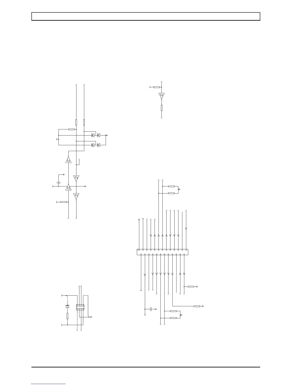
MC-Bus, main PCB connectors
Main PCB schematic diagram
This link fitted only for Cyrus 6a
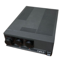
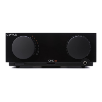
Cyrus 6 DAC, Cyrus 8 DAC amplifier service manual Issue 1© Cyrus Audio Ltd Jun 2014
44