SF600/SF600
Plus
Serial Flash Programming solution
www.dediprog.com 20
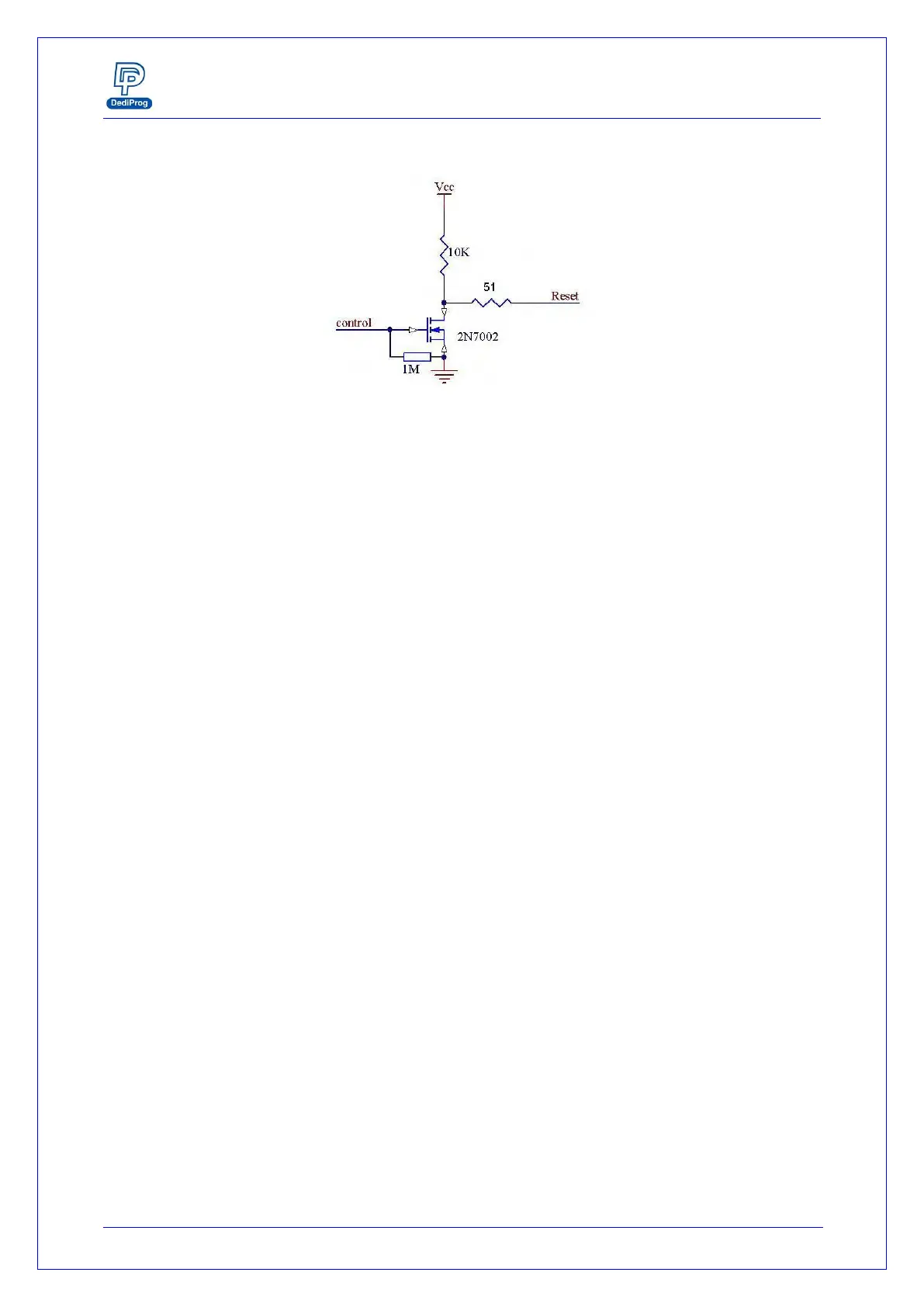
Fig 11: Circuit diagram:
IO: The IO signals are in input mode by default. Behavior to be customized.
For the DC characteristics of IO1 and IO2 please refer to the DC table.
ESD high performance protection compliant with IEC61000-4-2 level 4: 15kV
(air discharge) 8kV( contact discharge)
5.2.3 ICP timing
The IO and reset have been designed to set the application in programming mode
before applying the SPI signal. They can be used to reset the target application, to turn
OFF MOSFET and isolate the SPI bus when programmer is working.
A. If No programmer operation is on going
All our SF600 and SF600Plus outputs are equivalent to high impedance.
B. When an operation is requested on the user interface
- IO1, IO2 are kept in Input by default (High Impedance)
- Reset/IO3 signals are driven Low.
C. 3 ms after Reset is switched to Low Impedance, the SPI outputs are switched in
low impedance too.
- CS1 and CS2 are driven high
- Clock and MOSI are driven low
- DQ0-3 are driven low if Quad IO outputs is enable
- Hold, Wp are driven High if single IO mode is used
D. The programmer is then ready for the communication with the Serial Flash.
So designer can use the Reset signal to reset or switch the application Serial bus in
High impedance. Application controller or circuitry will have a delay of 3ms
between Reset is driven low and Programmer SPI outputs are switched from High
Impedance to Low Impedance. SPI communication starts 6ms after reset has been
driven low.