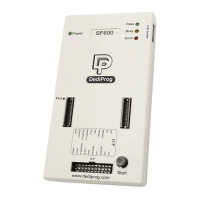
SF600/SF600
Plus
Serial Flash Programming solution
www.dediprog.com 7
Table 4: Description of the signals:
High voltage applied on the SPI Flash to speed up the
programming and erasing operations.
Chip select of two Serial Flashes. Serial Flash 1 or 2 can be
selected from the software.
Vcc is used to supply the application SPI Flash. The Vcc level
can be adjusted from the software. A diode protects the
SF600/SF600Plus Vcc from the application Vcc.
Data out from the application memory (master in slave out)
when memory work in single IO mode. Bi-directional when
memory works in Dual or Quad IO mode.
Driven High when Hold function is active. Bi-directional when
memory works in Quad IO mode.
Driven High when Wp function is active. Bi-directional when
memory works in Quad IO mode.
GND is the common ground shared between application and
programmer
Data in of the application SPI Flash (master out slave in)
when memory work in single IO mode. Bi-directional
when memory works in Dual or Quad IO mode.
Open drain output driven low prior any SF600/SF600Plus
operation. Reset/IO3 can be used to turn on the application
isolation circuit or reset the target system in order to drive the
Serial bus in High Impedance.
11, 13,
14, 15,
16, 17,
18
General I/O can be used for customization.