18
AVR-4802/AVC-A11SR
1
2
3
4
5
6
7
8
16
15
14
13
9
10
11
12
20
19
18
17
V
DD1
VERT*
HOR*
OSCIN
OSCOUT
P3
P2
P1
P0
Vss
OSC1
OSC2
CS
SCK
SIN
AC
V
DD2
CVIDEO
LECHA
CVIN
3
4
5
20
6
11
7
1
2
19 18
17
16
8
9
10
12
13
14
15
CS
SCK
SIN
V
DD1
AC
V
SS
V
DD2
OSCI
OSC2
VERT*
HOR*
INPUT
CONTROL
CIRCUIT
DATA
CONTROL
CIRCUIT
ADDRESS
CONTROL
CIRCUIT
INDICATION
OSCILLATOR
TIMING
GENERATOR
INDICATION
CONTROL
REGISTER
INDICATION RAM
INDICATION CHARACTER ROM
BLINKING CIRCUIT
SYNC SIGNAL
SWITCHING CIRCUIT
H COUNTER
INDICATION LOCATION
DETECTION CIRCUIT
READ OUT ADDRESS
CONTROL CIRCUIT
INDICATION
CONTROL CIRCUIT
SHIFT REGISTER
SYNC SIGNAL DIS-
CRIMINATING CIRCUIT
OSC CIRCUIT
FOR SYNC SIGNAL
GENERATION
TIMING
GENERATOR
NTSC
VIDEO OUTPUT
CIRCUIT
OSCIN
OSCOUT
CVIDEO
LECHA
CVIN
P0
P1
P2
P3
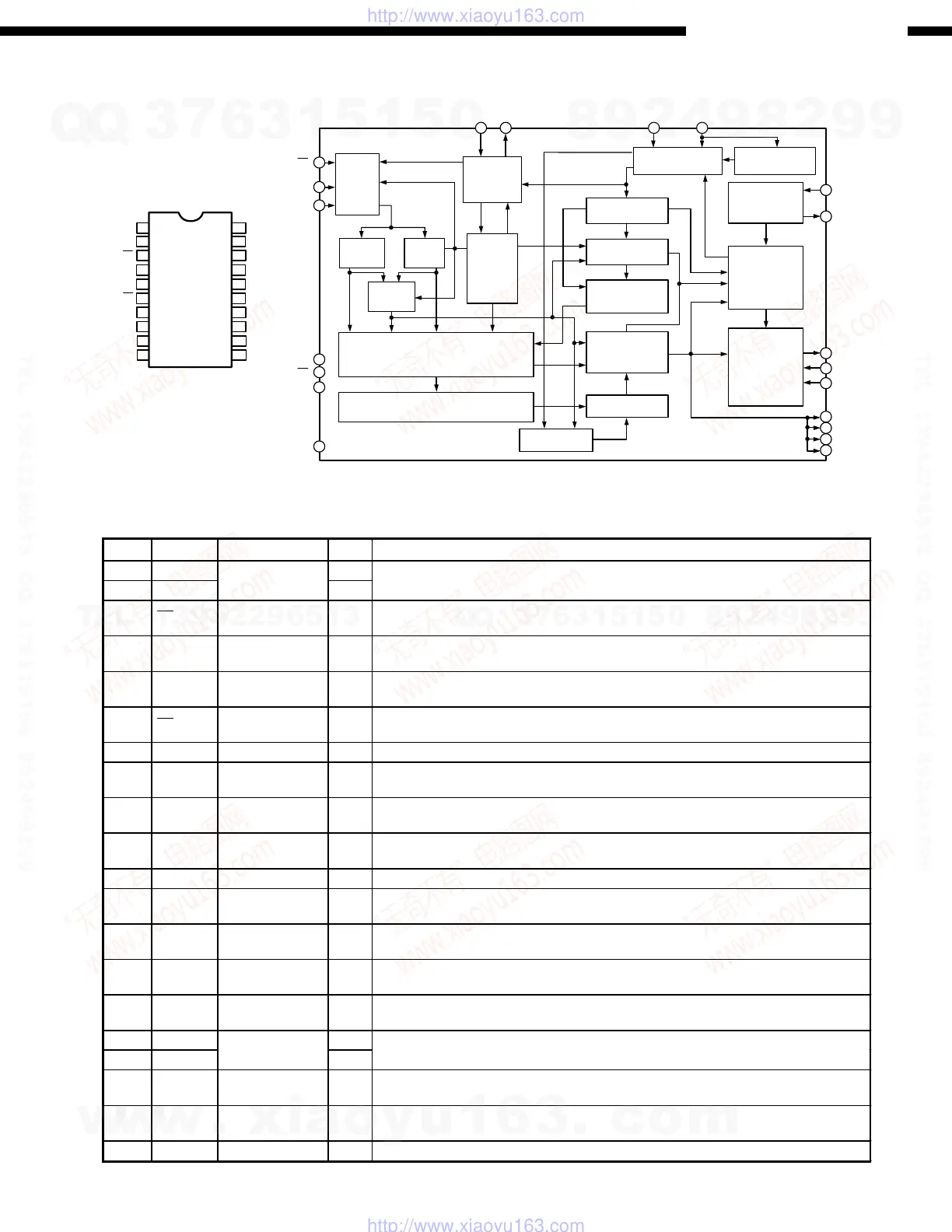
M35015-210SP (IC416)
M35015-210SP Terminal Function
Pin No. Symbol Name I/O Function
1 OSC1 Osc. circuit ext. I External terminal for indication oscillator circuit. Standard OSC. freq. is approx. 7MHz.
2 OSC2 terminal. O With this OSC. freq., decides horizontal indicatin and character width.
3 CS Chip select input I
Chip select terminal and turns to “L” when transfer serial data.
Hysteresis input. Pull up resistor is built-in.
4 SCK Serial clock input I
Takes in serial data of SIN at SCK rise when CS terminal is in “L”.
Hysteresis input. Pull up rersist is built-in.
5 SIN Serial data input I
Serial input of register for indication control and data, and address for indication data
memory. Hysteresis input. Pull up rersistor is built-in.
6 AC Auto-clear input I
Resets internal circuit of IC at “L” mode.
Hysteresi input. Pull up resistor is built-in.
7V
DD2
Power supply
Power supply terminal of analog system. Connect to +5V.
8CVIDEO
Combined
video output
O
Output terminal of combined video signal. Outputs 2Vp-p combined signal. Character
output, etc. Overlap CVIN signal and outputs at superimpose.
9 LECHA
Character level
input
I
Input terminal deciding character output level in combined video signal. color of character
is white.
10 CVIN
Combined video
input
I
Input terminal of external combined video signal.
Character output etc. overlap this external combined video signal.
11 Vss Ground
Ground terminal. Connect to GND.
12 P0 Output port p0 O
General output or character background signal BL NK1* output is switchable.
Polarity can be selected at ROM mask.
13 P1 Output port P1 O
General output or character background signal CO1* output is switchable.
Polarity can be selected at ROM mask.
14 P2 Output port P2 O
General output or character background signal BLNK2* output is switchable.
Polarity can be selected at ROM mask.
15 P3 Output port P3 O
General output or character background signal CO2* output is switchable.
Polarity can be selected at ROM mask.
16 OSCOUT O Terminal for external use of sync si
nal OSC. circuit. Use the freq.: 14.32MHz at NTSC
17 OSCIN I system, 17.73MHz at PAL. system, 14.30MHz at MPAL system.
18 HOR*
Horizontal sync
signal
I
Inputs horizontal sync signal.
Hysteresis input.
19 VERT*
Vertical sync
signal
I Input vertical sync signal. Hysteresis input. Polarity can be selected at ROM mask.
20 V
DD1
Power supply
Power supply terminal of digital system. Connect to +5V.
Ext. terminal
for sync sig.
OSC. Circuit
w
w
w
.
x
i
a
o
y
u
1
6
3
.
c
o
m
Q
Q
3
7
6
3
1
5
1
5
0
9
9
2
8
9
4
2
9
8
T
E
L
1
3
9
4
2
2
9
6
5
1
3
9
9
2
8
9
4
2
9
8
0
5
1
5
1
3
6
7
3
Q
Q
TEL 13942296513 QQ 376315150 892498299
TEL 13942296513 QQ 376315150 892498299
http://www.xiaoyu163.com
http://www.xiaoyu163.com
 Loading...