TERMINAL
I/O
PULL-
DOWN
5-V
TOLERANT
DESCRIPTION
NAME PIN
VOUT1+ 43 O No No Positive analog output from DAC1
VOUT1- 44 O No No Negative analog output from DAC1
RSV2 45 — — — Reserved, tied to analog ground
AGND2 46 — — — Analog ground 2
VCC2 47 — — — Analog power supply 2, +5 V
RSV2 48 — — — Reserved, tied to analog ground
(1) Open-drain conguration in out mode.
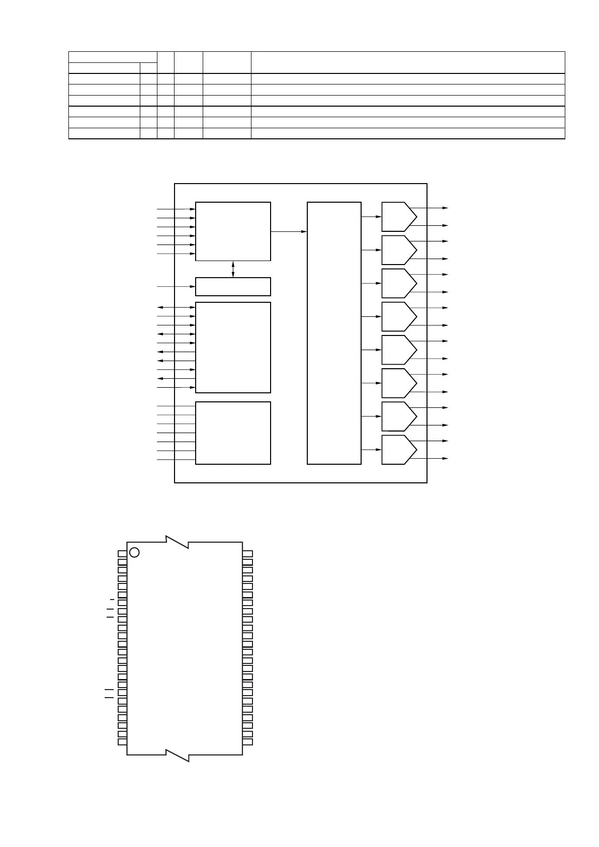
PCM1690 FUNCTIONAL BLOCK DIAGRAM
H27U1G8F2BTR-BC (DIGITAL : IC394)
DAC
VOUT1
DAC
VOUT2
DAC
VOUT3
DAC
VOUT4
DAC
VOUT5
DAC
VOUT6
AGND2
VDD
DGND
VCOM
VCC1
AGND1
VCC2
DAC
VOUT7
DAC
VOUT8
DigitalFilter
and
Volume
PowerSupplyand
CommonVoltage
SCKI
SCKManager
RST
AMUTEO
AMUTEI
ZERO2
ZERO1
MODE
MD/SDA/DEMP
MC/SCL/FMT
MS/ADR0/RSV
ControlInterface
(SPI/I C/HW)
2
LRCK
BCK
DIN4
DIN3
DIN2
DIN1
AudioInterface
PCM1690
SBAS448A–OCTOBER 2008– REVISED JANUARY 2009..............................................................................................................................................
www.ti.com
8 Submit Documentation Feedback Copyright © 2008–2009, Texas Instruments Incorporated
Product Folder Link(s): PCM1690
Rev 1.1 / Sep. 2009 5
1
H27U1G8F2B Series
1 Gbit (128 M x 8 bit) NAND Flash
VCC
VSS
WP
CLE
ALE
RE
WE
CE IO0~IO7
R/B
NC
NC
NC
NCNC
NC NC
NC
CLE
ALE Vss
Vss
Vss
Vcc
Vcc
NC
NC
NC
WP
RE
CE
WE RB
NC
NC
NC
NC
NC
NC
NC
NC
NC
NC
NC
NC
NC
I/O0
I/O1
I/O9
I/O2
I/O3
I/O10
I/O11
I/O4
I/O15
I/O12 I/O14
I/O13
I/O6
I/O7 I/O5
NC
NC NC NC
NC
PRE
I/O8
NC
NCNC
NC NC
A
B
C
D
E
F
G
H
J
K
L
M
1 2 3 4 5 6 7 8 9 10
uhukGm
GGGGminh
GGGGGO_P
Figure 2 : 48-TSOP1 / 63-FBGA Contact, x8 Device
IO7 - IO0 Data Input / Outputs
CLE Command latch enable
ALE Address latch enable
CE Chip Enable
RE Read Enable
WE Write Enable
WP Write Protect
R/B
Ready / Busy
Vcc Power Supply
Vss Ground
NC No Connection
Figure 1 : Logic Diagram Table 1 : Signal Names
1&
1&
1&
1&
1&
1&
5%
5(
&(
1&
1&
9FF
9VV
1&
1&
&/(
$/(
:(
:3
1&
1&
1&
1&
1&
1&
1&
1&
1&
,2
,2
,2
,2
1&
1&
1&
9FF
9VV
1&
1&
1&
,2
,2
,2
,2
1&
1&
1&
1&
1$1')ODVK
7623
[
183
 Loading...