15
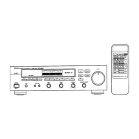
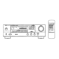
DRA-397/297/37
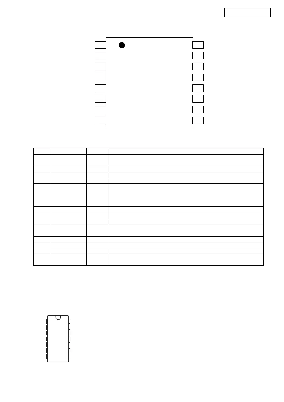
AK4385 (IC 207) XM-READY P.W.B.
SN74LV08A (IC 204) XM-READY P.W.B.
SN74HCT08 (IC 205, 206, 211) XM-READY
1
MCLK
LRCK
BICK
CSN
CCLK
CDTI
Top
View
2
3
4
5
6
7
8
DZFL
DZFR
VSS
VDD
AOUTL+
AOUTL-
AOUTR+
AOUTR-
16
15
14
13
12
11
10
9
PDN
SDTI
No. Pin Name I/O Function
1 MCLK I Master Clock Input Pin
An external TTL clock should be input on this pin.
2 BICK I Audio Serial Data Clock Pin
3 SDTI I Audio Serial Data Input Pin
4 LRCK I L/R Clock Pin
5 PDN I Power-Down Mode Pin
When at “L”, the AK4385 is in the power-down mode and is held in reset.
The AK4385 should always be reset upon power-up.
6 CSN I Chip Select Pin
7 CCLK I Control Data Input Pin
8 CDTI I Control Data Input Pin
9 AOUTR- O Rch Negative Analog Output Pin
10 AOUTR+ O Rch Positive Analog Output Pin
11 AOUTL- O Lch Negative Analog Output Pin
12 AOUTL+ O Lch Positive Analog Output Pin
13 VSS - Ground Pin
14 VDD - Power Supply Pin
15 DZFR O Rch Data Zero Input Detect Pin
16 DZFL O Lch Data Zero Input Detect Pin
Note: All input pins should not be left floating.
Pin function
1
2
3
4
5
6
7
14
13
12
11
10
9
8
1A
1B
1Y
2A
2B
2Y
GND
V
CC
4B
4A
4Y
3B
3A
3Y