SERVICE MANUAL
MODEL
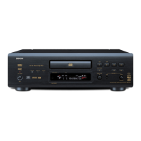
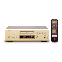
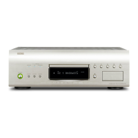
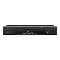
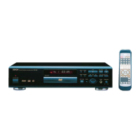
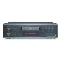
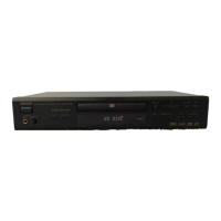
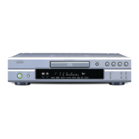
DVD-5900
DVD-A11
DVD AUDIO-VIDEO / SUPER AUDIO CD PLAYER
For U.S.A., Canada, Europe
& Japan model
16-11, YUSHIMA 3-CHOME, BUNKYOU-KU, TOKYO 113-0034 JAPAN
X0176V.02 DE/CDM 0310
注 意
サービスをおこなう前に、このサービスマニュアルを
必ずお読みください。本機は、火災、感電、けがなど
に対する安全性を確保するために、さまざまな配慮を
おこなっており、また法的には「電気用品安全法」に
もとづき、所定の許可を得て製造されております。
従ってサービスをおこなう際は、これらの安全性が維
持されるよう、このサービスマニュアルに記載されて
いる注意事項を必ずお守りください。
● 本機の仕様は性能改良のため、予告なく変更すること
があります。
● 補修用性能部品の保有期間は、製造打切後
8年です。
Some illustrations using in this service manual are
slightly different from the actual set.
●
●
Please use this service manual with referring to
the operating instructions without fail.
●
For purposes of improvement, specifications and
design are subject to change without notice.
●
修理の際は、必ず取扱説明書を参照の上、作業を行って,
ください。
● 本文中に使用しているイラストは、説明の都合上現物
と多少異なる場合があります。
Ver. 2
w
w
w
.
x
i
a
o
y
u
1
6
3
.
c
o
m
Q
Q
3
7
6
3
1
5
1
5
0
9
9
2
8
9
4
2
9
8
T
E
L
1
3
9
4
2
2
9
6
5
1
3
9
9
2
8
9
4
2
9
8
0
5
1
5
1
3
6
7
3
Q
Q
TEL 13942296513 QQ 376315150 892498299
TEL 13942296513 QQ 376315150 892498299
http://www.xiaoyu163.com
http://www.xiaoyu163.com