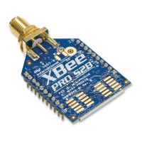
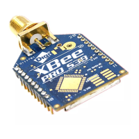
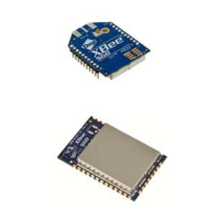
XBee® Wi-Fi RF Modules
© 2013 Digi International, Inc. 117
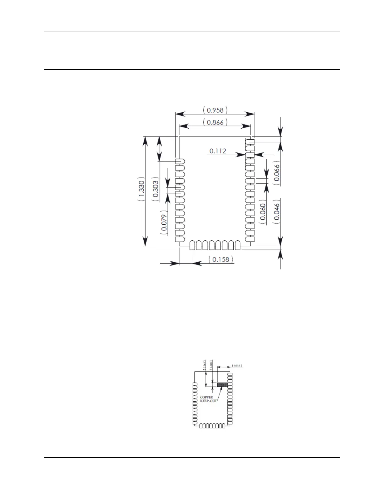
Recommended Footprint
It is recommended that you use the PCB footprint shown below for surface mounting.
Dimensions are in inches.
The solder footprint should be matched to the copper pads, but may need to be
adjusted depending on the specific needs of assembly and product standards. While the
underside of the module is mostly coated with solder resist, it is recommended that the
copper layer directly below the module be left open to avoid unintended contacts.
Copper or vias must not interfere with the three exposed RF test points on the bottom
of the module (see below). Furthermore, these modules have a ground plane in the
middle on the back side for shielding purposes, which can be affected by copper traces
directly below the module.
 Loading...