Mapping of I/O Signals
▲
■■■■■■■■■■■■■■■■■■■■■■■■■■■■■■■■■■■■■■■■■■■■■■■■■■■■■■■■■■■■■■■■■■■■■■■■■■■■■■■■■■■■■■■■■■■■■■■■
DS1104 Hardware Installation and Configuration March 2004
I■■■■■■■■■■■■■
▼
108
■■■■■■■■■■■■■■■▼
VCC pins The following I/O pins provide access to the PC power supply VCC
(+5 V):
N
■ For the DS1104, the total load of the connector pins P1 19 and
P1 20 (pins P1B 4 and P1A 4 on the Sub-D connector) must not
exceed 500 mA.
■ For the connector panels CP1104 and CLP1104, the total load of
all connector pins that provide access to the PC power supply must
not exceed 500 mA (CP1104) or 400 mA (CLP1104).
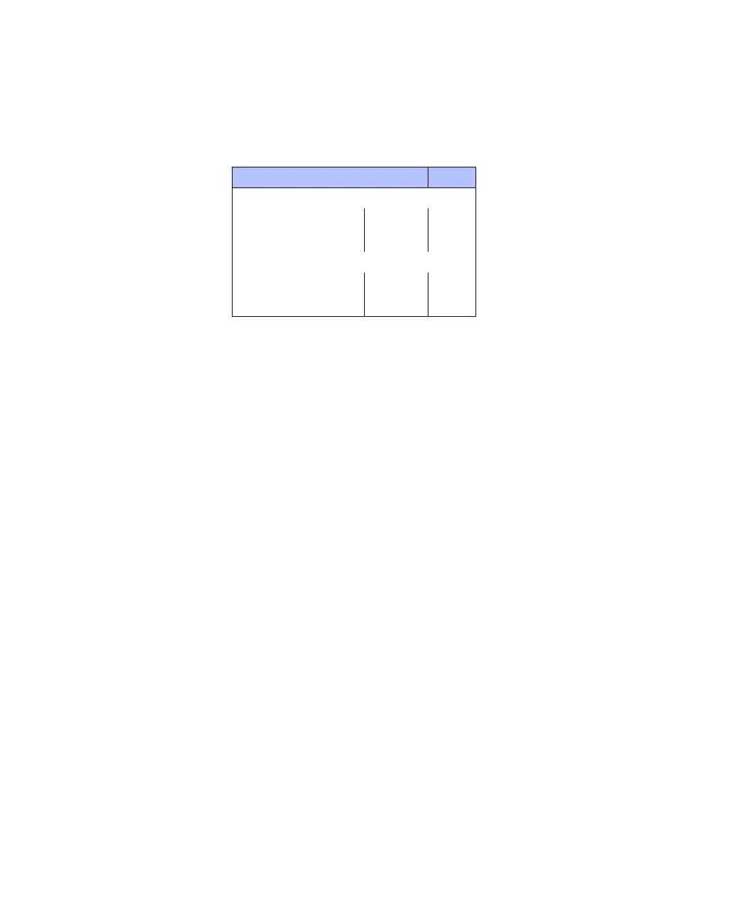
Connector Pin
DS1104
I/O Connector P1 19, 20
Sub-D Connector P1A 4
P1B 4
CP1104/CLP1104 Connector Panel
Digital I/O CP17 36, 37
Slave I/O CP18 18, 19
Incremental Encoder Interface CP19, CP20 1, 9