EasyManuals Logo

Epson RX8111CE User Manual

Epson RX8111CE
67 pages
To Next Page IconTo Next Page
To Previous Page IconTo Previous Page
Page #21 background imageLoading...
Page #21 background image
RX8111CE
Page17
ETM61E-01
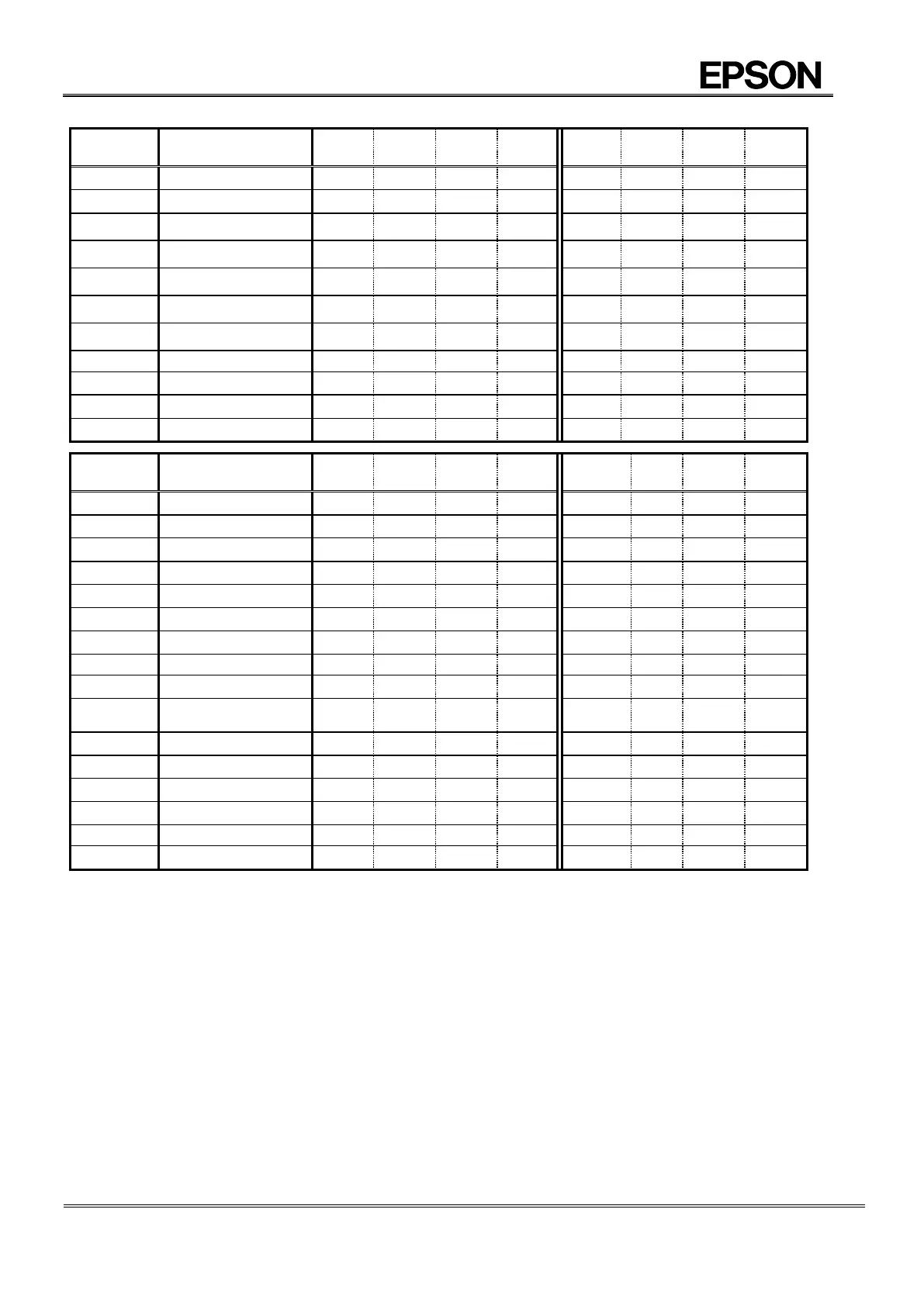
Table 10 Register Table (2)
Address
Function
bit 7
bit 6
bit 5
bit 4
bit 3
bit 2
bit 1
bit 0
30h
No Function
z
z
z
z
z
z
z
z
31h
No Function
z
z
z
z
z
z
z
z
32h
Power Switch Control
CHGEN
INIEN
z
z
SWSEL1
SWSEL0
SMPT1
SMPT0
33h
Status Monitor
z
EVIN
z
z
VCMP
z
VLOW
z
34h
Time Stamp Control 1
z
z
z
z
z
EISEL
TSCLR
TSRAM
35h
Time Stamp Control 2
z
z
z
ECMP
EVDET
EVLOW
EXST
36h
Time Stamp Control 3
z
z
z
TSFULL
TSEMP
TSAD2
TSAD1
TSAD0
37h
No Function
z
z
z
z
z
z
38h - 3Dh
No Function
z
z
z
z
z
z
z
z
3Eh
No Function
-
-
-
-
-
-
-
-
3Fh
TEST
TEST
z
z
z
z
z
z
z
Address
Hex
Function
bit 7
bit 6
bit 5
bit 4
bit 3
bit 2
bit 1
bit 0
40,50,60,70
Time stamp 1/256 s
1/2
1/4
1/8
1/16
1/32
1/64
1/128
1/256
41,51,61,71
Time Stamp SEC
40
20
10
8
4
2
1
42,52,62,72
Time Stamp MIN
40
20
10
8
4
2
1
43,53,63,73
Time Stamp HOUR
20
10
8
4
2
1
44,54,64,74
Time Stamp DAY
20
10
8
4
2
1
45,55,65,75
Time Stamp MONTH
10
8
4
2
1
46,56,66,76
Time Stamp YEAR
80
40
20
10
8
4
2
1
47,57,67,77
Status stamp
VLOW
VCMP
VDET
XST
48,58,68,78
Time stamp 1/256 s
1
2
4
8
16
32
64
128
49,59,69,79
Time Stamp SEC
40
20
10
8
4
2
1
4A,5A,6A,7A
Time Stamp MIN
40
20
10
8
4
2
1
4B,5B,6B,7B
Time Stamp HOUR
20
10
8
4
2
1
4C,5C,6C,7C
Time Stamp DAY
20
10
8
4
2
1
4D,5D,6D,7D
Time Stamp MONTH
10
8
4
2
1
4E,5E,6E,7E
Time Stamp YEAR
80
40
20
10
8
4
2
1
4F,5F,6F,7F
Status stamp
VLOW
VCMP
VDET
XST
After the initial power-up (from 0 V) or in case the VLF bit returns "1", make sure to initialize all registers, before using the RTC.
The TEST bit (3Fh bit7) is used by the manufacturer for testing. Be sure to set "0" for this bit when writing.
Be sure to write "0" by initializing before using the clock module. Afterward, be sure to set "0" when writing.
Be sure to avoid entering incorrect date and time data, as clock operations are not guaranteed when the data or time data is incorrect.
Any bit marked with "z" should be used with a value of "0" after initialization. (Not writable)
Any bit marked with "" is a RAM bit that can be used to read or write any data.
Any bit marked wit' -- 'is Not writable. Read result is unkown.
The above table shows only the user registers. Due to functional reasons, RTC has different registers not mentioned above table which
are programmed by the manufactorer. Please make sure to only access above mentioned user registers.
Even if it is done Read/Write access as for “No Function”, a function else has no influence.
When not using Week data, It is not necessary for Week register to be initialized.
By read/write to register of No-Function, other functions are not affected.

Table of Contents

Questions and Answers:

Question and Answer IconNeed help?

Do you have a question about the Epson RX8111CE and is the answer not in the manual?

Epson RX8111CE Specifications

General IconGeneral
BrandEpson
ModelRX8111CE
CategoryControl Unit
LanguageEnglish

Related product manuals