EasyManuals Logo

Epson RX8111CE User Manual

Epson RX8111CE
67 pages
To Next Page IconTo Next Page
To Previous Page IconTo Previous Page
Page #20 background imageLoading...
Page #20 background image
RX8111CE
Page16
ETM61E-01
13.2. Register Table
13.2.1. Register Table
Table 9 Register Table (1)
Address
Hex
Function
bit 7
bit 6
bit 5
bit 4
bit 3
bit 2
bit 1
bit 0
10
SEC
z
40
20
10
8
4
2
1
11
MIN
z
40
20
10
8
4
2
1
12
HOUR
z
z
20
10
8
4
2
1
13
WEEK
z
6
5
4
3
2
1
0
14
DAY
z
z
20
10
8
4
2
1
15
MONTH
z
z
z
10
8
4
2
1
16
YEAR
80
40
20
10
8
4
2
1
17
MIN Alarm
AE
40
20
10
8
4
2
1
18
HOUR Alarm
AE
20
10
8
4
2
1
19
WEEK Alarm
AE
6
5
4
3
2
1
0
DAY Alarm
20
10
8
4
2
1
1A
Timer Counter 0
128
64
32
16
8
4
2
1
1B
Timer Counter 1
32768
16384
8192
4096
2048
1024
512
256
1C
Timer Counter 2
8388608
4194304
2097152
1048576
524288
262144
131072
65536
1D
Extension Register
FSEL1
FSEL0
USEL
TE
WADA
ETS
TSEL1
TSEL0
1E
Flag Register
POR
z
UF
TF
AF
EVF
VLF
XST
1F
Control Register
z
z
UIE
TIE
AIE
EIE
z
STOP
Address
Function
bit 7
bit 6
bit 5
bit 4
bit 3
bit 2
bit 1
bit 0
20h
Time Stamp 1/1024S
--
--
--
--
--
--
1/512
1/1024
21h
Time Stamp 1/256S
1/2
1/24
1/8
1/16
1/32
1/64
1/128
1/256
22h
Time Stamp SEC
z
40
20
10
8
4
2
1
23h
Time Stamp MIN
z
40
20
10
8
4
2
1
24h
Time Stamp HOUR
z
z
20
10
8
4
2
1
25h
Time Stamp WEEK
z
6
5
4
3
2
1
0
26h
Time Stamp DAY
z
z
20
10
8
4
2
1
27h
Time Stamp MONTH
z
z
z
10
8
4
2
1
28h
Time Stamp YEAR
80
40
20
10
8
4
2
1
29h
Status Stamp
z
z
VLOW
VCMP
VDET
z
XST
z
2Ah
No Function
z
z
z
z
z
z
z
z
2Bh
EVIN Setting
EHL
ET1
ET0
PDN
PU1
PU0
OVW
-
2Ch
SEC Alarm
AE
40
20
10
8
4
2
1
2Dh
Timer Control
z
z
z
z
TBKON
TBKE
TMPIN
TSTP
2Eh
Time Stamp control 0
z
z
z
z
z
z
z
COMTG
2Fh
Command Trigger
z
z
z
z
z
z
z
z
After the initial power-up (from 0 V) or in case the VLF bit returns "1" , make sure to initialize all registers, before using the RTC.
Be sure to avoid entering incorrect date and time data, as clock operations are not guaranteed when the data or time data is incorrect.
Any bit marked with "z" should be used with a value of "0" after initialization. (Not writable)
Any bit marked with "" is a RAM bit that can be used to read or write any data.
Any bit marked with' -- 'is Not writable. Read result is unkown.
The above table shows only the user registers. Due to functional reasons, RTC has different registers not mentioned above table which are
programmed by the manufactorer. Please make sure to only access above mentioned user registers.
By read/write to register of No-Function, other finction are not affected.
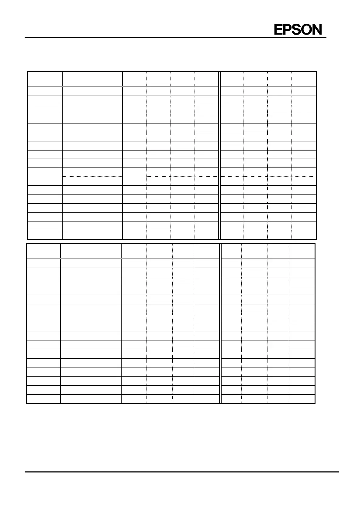
Table of Contents

Questions and Answers:

Question and Answer IconNeed help?

Do you have a question about the Epson RX8111CE and is the answer not in the manual?

Epson RX8111CE Specifications

General IconGeneral
BrandEpson
ModelRX8111CE
CategoryControl Unit
LanguageEnglish

Related product manuals