14.7. Battery backup switchover function
14.7.1. Description of Battery backup switchover function
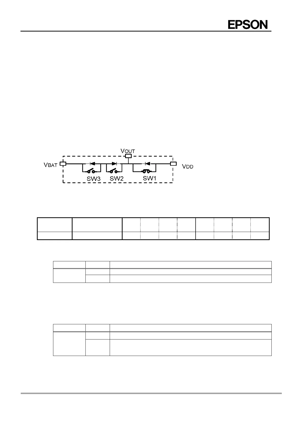
There are three kinds of detection, switchover functions.
1) V
DD
voltage detection (VDET) comparison between V
DD
voltage and V
DET1
(INIEN register control)
2) V
BAT
recharge detection (VCMP) comparison between V
BAT
voltage and V
DD
voltage (CHGEN register control).
3) V
BAT
voltage detection (VLOW) comparison between V
BAT
voltage and V
LOW
voltage (EVLOW register control)
V
DD
voltage detection and V
BAT
recharge detection are shown in Figure 31 and Figure 32.
The detection, switchover function is composed from diodes ,switch and comparator between V
DD
and V
BAT
.
The RTCs backup function is built in a way to prevent reverse current flow from V
BAT
to V
DD
.
There are two kinds of operation modes:
1) Normal mode power supply from V
DD
2) Backup mode power supply from V
BAT
In backup mode FOUT pin becomes Hi-Z, I
2
C input enable (SDA, SCL: Hi-Z).
VLF detection (VLF bi”0” → “1)makes battery backup switchover related register to default.
Figure 26 Battery Backup switchover function block diagram
14.7.2. Battery backup switchover related register
Table 44 Battery backup switchover related register
To set CHGEN active User should set INIEN to “1”.
2) INIEN bit (Initial Enable)
By setting INIEN to “1” automatic MOS SW control works and CHGEN bit control becomes available
When INIEN bit is “1”, I
2
C bus active/inactive control is available based on comparison result V
DD
and V
DET1
.
Table 46 INIEN bit (Initial Enable)
CHGEN bit setting become active.
VDD voltage low detection makes I
2
C bus inactive and SDA,SCL become Hi-
Z.
3) INIEN bit (Initial Enable)
This bit is used for enabling/disabling VLOW function as well as for controlling time stamp operation.
(Please refer to 14.8.6 for the detail)
Battery Backup Switchover control (Initial power on)